Can Photonics Break AI’s Memory Wall? Optical Interconnect vs. Photonic Memory and In-Memory Optical Computing
Why optical interconnect, not photonic memory or optical compute, is the investable fix for AI’s memory wall, with Marvell, Nvidia, and Lightmatter.

What Happens When Memory Stops Being a Separate Device? Optical Delay, Recurrent Photonic State, Nonvolatile Photonic Memory, and the Convergence of Storage and Computation
1. Summary
The nearer-term investable value in photonics lies overwhelmingly in near-memory and memory-disaggregation optics, not in true in-memory photonic computing or in optical storage of data. The evidence for this is now unambiguous in the capital markets: Marvell (NASDAQ:MRVL) completed its acquisition of Celestial AI on February 2, 2026 for a total purchase consideration of $3.5 billion, Nvidia (NASDAQ:NVDA) committed $4 billion (roughly $2 billion each) across Coherent (NYSE:COHR) and Lumentum (NASDAQ:LITE) on March 2, 2026, and Ayar Labs closed a $500 million Series E on March 3, 2026 at a $3.75 billion valuation. Every one of these transactions funds optical interconnect that moves conventional electronic memory closer to compute; none of them funds a product that stores or computes on data in the optical domain.
The physics explains why. Photons do not sit still, so optical delay cannot serve as dense, addressable memory: delay-line capacity scales as bandwidth times delay and is capped by the delay-bandwidth product, propagation loss, and footprint, limiting integrated buffers to nanoseconds and a handful of bits rather than the megabytes a compute engine needs. Recurrent photonic state (reservoir computing) remains a laboratory technique validated on synthetic benchmarks, not commercial workloads. Nonvolatile photonic memory using phase-change materials is improving, with demonstrations of 4 to 7 bits per cell and low insertion loss, but it is gated by endurance (often only thousands of cycles on-chip), multilevel drift, and per-cell write energies in the nanojoule-to-microjoule range that make it unsuitable as a general memory tier.
True in-memory photonic computing crossed an important threshold in April 2025, when Lightmatter reported a packaged photonic processor running ResNet, BERT and reinforcement-learning models at near-electronic precision with system-level energy accounting. This is the most credible photonic-compute result to date, but it competes against a fast-moving electronic bar (HBM4, processing-in-memory DRAM, and analog compute-in-memory) and its advantage is throttled by the conversion overhead that dominates every hybrid optoelectronic system. The investor's conclusion: allocate to interconnect and packaging now, treat photonic compute as a venture-stage option, and treat optical data storage as a research curiosity.
2. Background
The binding constraint in AI hardware has shifted from arithmetic to data movement. Micron's HBM Design Architecture Fellow Raghu Sreeramaneni told Hot Chips 2026 that compute throughput is scaling at roughly 3x every two years while HBM bandwidth scales at closer to 2x every two years, so the "memory wall" is still present and, in his words, "maybe getting worse." In a typical GPU system-in-package with four 12-high HBM4 stacks, memory accounts for approximately 90 percent of the silicon (about 8x the GPU die area), and moving parameters between memory and compute cores consumes a substantial share of both time and energy in large-model inference. The industry response, visible across the Micron, Samsung and SK hynix roadmaps, is to bring memory physically and electrically closer to compute through advanced packaging, hybrid bonding, and now optical links.
Optics is proposed as a remedy for two distinct reasons that must not be conflated. First, light moves data at very high bandwidth density and low energy per bit over distance, which is an interconnect argument. Second, light can in principle perform linear algebra (the multiply-accumulate operations that dominate AI) as it propagates, which is a computation argument. A third, more speculative idea is that light could also hold state, either transiently in a delay or feedback loop or persistently in a switchable material, so that the memory and the processor stop being separate devices. This report evaluates all three claims (delay, recurrence, nonvolatile memory) and both convergence levels (true in-memory compute versus near-memory interconnect), and asks which is investable and when.
3. Key Players
The players that bear on the investment thesis divide cleanly into optical interconnect (where money and revenue are accruing) and optical compute or memory (where the science is maturing but revenue is thin).
In interconnect, Celestial AI is the most consequential recent event. Its Photonic Fabric platform, which the company claims delivers 25 times the bandwidth at 10 times lower latency than co-packaged optics alternatives and can deliver optically encoded data to any point on a compute die rather than only its edge, was acquired by Marvell. Marvell's FY2026 10-K discloses that the deal closed February 2, 2026 with approximately $1.3 billion in cash and roughly 24.5 million shares issued at close, plus revenue-milestone earnouts through fiscal 2029; press reporting put the headline upfront value at $3.25 billion and the maximum including earnouts at $5.5 billion. Lightmatter, still private, had raised $850 million at a $4.4 billion valuation as of its October 2024 Series D led by T. Rowe Price, and markets its Passage 3D photonic interposer with a claimed 114 Tbps of total optical bandwidth. Ayar Labs, also private, raised its $500 million Series E (led by Neuberger Berman) at a $3.75 billion valuation, bringing total funding to about $870 million, with strategic backing from Nvidia, AMD, MediaTek and Alchip; its TeraPHY optical I/O chiplet is specified at up to 8 Tbps bidirectional and roughly 5 pJ per byte. Nvidia's $4 billion split investment in Coherent and Lumentum ($2 billion each, in nonexclusive multiyear agreements with multibillion-dollar purchase commitments) signals that the GPU incumbent regards the optical supply chain, including lasers and indium phosphide, as a strategic bottleneck. Broadcom (NASDAQ:AVGO), Marvell and Intel (NASDAQ:INTC) run their own co-packaged optics programs. POET Technologies (NASDAQ:POET) is a small-cap optical-interposer designer, still early-stage with limited revenue and a fab-light model. iPronics (Spain) is a small programmable-photonics startup at Series A scale.
In compute and memory, the players are earlier and mostly European. Q.ANT (Germany, a Trumpf spin-off) raised a €62 million Series A in July 2025 (roughly $80 million total funding) and ships a thin-film lithium niobate photonic co-processor it claims runs at 30 W with large energy and performance multipliers versus GPUs; these are company claims and independent workload verification is limited. Lightmatter also pursues photonic compute (its Envise processor and the 2025 Nature demonstration). Lightelligence (MIT spin-out) builds optical-interposer AI compute. Salience Labs (UK) and Akhetonics (Germany, which raised a roughly €6 million seed in 2024 and pursues all-optical logic including optical memory) are seed-to-early stage. The academic groups that anchor the field are the Bhaskaran group at Oxford, the Pernice group at Münster/Heidelberg, and their collaborators at Exeter, Karlsruhe, EPFL/IBM Zürich (barium titanate) and George Washington University (photonic tensor cores).
The direct competitors that define the bar photonics must clear are the memory and compute-in-memory incumbents. SK hynix, Samsung and Micron dominate HBM, with SK hynix holding roughly 58 percent of HBM revenue in the first quarter of 2026 (Counterpoint Research; IDC put it near 56 percent) and HBM4 entering production in 2026; HBM is sold out through 2026 and the market is projected to grow toward $100 billion by 2028. Processing-in-memory DRAM and analog electronic compute-in-memory (ReRAM, SRAM and eDRAM macros reported at tens to over a hundred TOPS/W at ISSCC and in Nature journals) are the electronic in-memory approaches that photonics must beat on a full-system basis. Foundries TSMC (NYSE:TSM), GlobalFoundries (NASDAQ:GFS), Tower Semiconductor (NASDAQ:TSEM) and Intel Foundry provide the silicon-photonics process access on which all of these startups depend.
4. Technical Considerations
4.1 Optical delay as memory
Optical delay cannot substitute for random-access memory because the stored quantity is a propagating field, not a static charge, and the amount of information a delay element can hold equals its bandwidth multiplied by its delay time. Resonant structures make this trade-off explicit: a single all-pass microring has a delay-bandwidth product near 2/π, so a 1 ns delay corresponds to only about 0.64 GHz of usable bandwidth, and coupled-resonator (CROW) chains that start with a delay-bandwidth product around 5 at low bit rates fall to unity as the data rate exceeds roughly 200 Gbps, while insertion loss compounds with every added resonator. Integrated waveguide spirals do better on bandwidth but pay in footprint and loss: a 2025 multimode silicon result achieved a record on-chip delay density (a 12.7 ns range in a 3.85 mm² footprint, with propagation losses of 0.2 to 0.49 dB/cm) that is impressive for microwave photonics and beamforming but still measures total capacity in nanoseconds and tens of bits, not the kilobits-to-megabits a compute tier requires. Architectures that break the delay-bandwidth constraint exist (parallel Mach-Zehnder topologies have shown 90 ps over more than 22 GHz), and free-space multipass cells reach very large time-bandwidth products (a nested Herriott-cell quantum-memory demonstration reported a time-bandwidth product of 3.87 x 10^7 with 687 ns delay at 95.4 percent transmission), but none of these delivers addressable, rewritable, dense storage. Optical delay is a useful buffering and synchronization primitive, not a memory technology.
4.2 Recurrent photonic state
Recurrent photonic state, in which the circulating optical field in a feedback loop is the memory, has been demonstrated repeatedly on benchmark tasks but not on commercially relevant workloads. Since the first silicon-photonics reservoir-computing chip in 2014, the field has shown chaotic time-series prediction (Santa Fe, Mackey-Glass), nonlinear channel equalization and isolated-word or speech recognition, and has pushed sampling times as low as 11.72 ps using semiconductor lasers under strong optical injection. Recent work continues to improve memory capacity and parallelism (deep and residual time-delay architectures, nonlinear-loop-mirror reservoirs, and integrated silicon-nitride true-time-delay elements inside the feedback loop). The consistent limitation is that these systems excel at low-dimensional temporal signal-processing tasks and have not been shown to run the dense, high-dimensional workloads (large transformers, convolutional classifiers at production accuracy) that drive AI economics. Reservoir computing is a niche edge-signal-processing technique, not a path to displacing the memory-compute hierarchy.
4.3 Nonvolatile photonic memory
Nonvolatile photonic memory is the most genuinely promising of the three state-holding mechanisms, but its device metrics still fall short of a deployable memory or weight-storage tier. Phase-change materials store information in the crystallinity of a chalcogenide film on a waveguide, read optically and written thermally or optically. The landmark 2015 demonstration achieved eight levels in a single cell with switching energies as low as 13.4 pJ near 1 GHz. Since then, low-loss transparent chalcogenides have improved the loss picture markedly: a GSSe (Ge2Sb2Se5) electrically programmed photonic RAM reported 4-bit operation with total insertion loss of 0.12 dB and modulation up to 0.2 dB/μm, and nitrogen-doped GST has reached over 7 bits (around 222 distinguishable levels) in a research device. The decisive weaknesses are endurance, drift and write energy. On-chip cycling endurance for photonic PCM has often been limited to roughly 1,000 cycles, improved to tens of thousands (about 67,000 with alumina encapsulation, around 50,000 in NASA microheater work) and, with nanostructured Sb2Se3, to more than 10^8 cycles but at write energies of 33 nJ for amorphization and 25 μJ for crystallization; Sb2Se3 also crystallizes slowly (millisecond-class pulses) and is intrinsically limited to roughly 10^3 to 10^5 cycles, versus 10^9 to 10^12 for bulk GST electronic memory. Retention is strong in principle (the GST amorphous state is stable for about ten years at 85 to 100 °C), but multilevel storage suffers resistance and optical drift: amorphous properties relax as a power law with a drift coefficient near 0.11 at room temperature, and the resistance distributions of an 11-level GST cell can begin to overlap within tens of seconds, corrupting the very multilevel encoding that in-memory computing depends on.
Alternative mechanisms partially sidestep these issues. Ferroelectric barium titanate offers non-volatile domain switching at roughly 80 ns with negligible holding power (a 2026 non-volatile BTO field-programmable photonic gate array integrated 58 unit cells and 116 actuators at 560 nW per π phase shift), and BTO microrings have shown eight-level storage stable beyond 12 hours at 0.191 pJ switching energy; but BTO devices remain physically large (millimeter-scale phase shifters) and are not yet a dense memory array. MEMS, charge-trapping and magneto-optic approaches remain at the individual-device research stage.
4.4 Convergence level (a): true in-memory photonic computing
True in-memory photonic computing, in which the stored optical state performs the arithmetic directly, has advanced from a physics demonstration to a system prototype but is not yet cost-competitive. The 2021 integrated photonic tensor core encoded matrix weights in PCM cells on waveguide crossings and is widely cited for tera-scale multiply-accumulate throughput, but that headline figure is a projection to the device's 14 GHz modulator bandwidth (a nominal 2 TMAC/s for a 9x4 matrix with four multiplexed inputs); the actual convolution in the paper ran at roughly 1 kHz, limited by the variable optical attenuators, and its efficiency figures are device-level, excluding the laser or comb source, the digital-to-analog and analog-to-digital converters, and the modulators. PCM photonic processors have also remained small, on the order of ten channels. The state of the art is Lightmatter's April 2025 Nature result: a package of four 128 x 128 photonic tensor cores plus digital control dies that generated 65.5 trillion adaptive-block-floating-point 16-bit operations per second at 78 W of electrical and 1.6 W of optical power (a system-level accounting that the authors stress had no prior end-to-end equivalent), running at a 500 MHz clock with a path to 2 GHz and 262 trillion operations per second.
In that system the data converters consume about 35.6 percent of power and the photonic tensor cores only 16.4 percent, which is itself the clearest illustration of where the energy actually goes. Crucially it achieved near-electronic accuracy on ResNet, BERT and Atari reinforcement learning without task-specific retraining for most workloads. This is the first photonic-compute result that competes with electronic accelerators on precision and honest energy, but the implied system efficiency (on the order of 0.8 operation per picojoule at the demonstrated clock) is not yet a decisive margin over leading electronic accelerators, and the weights here are electronically driven rather than stored optically, so this is analog optical compute rather than true nonvolatile in-memory compute.
4.5 Convergence level (b): near-memory and memory-disaggregation photonics
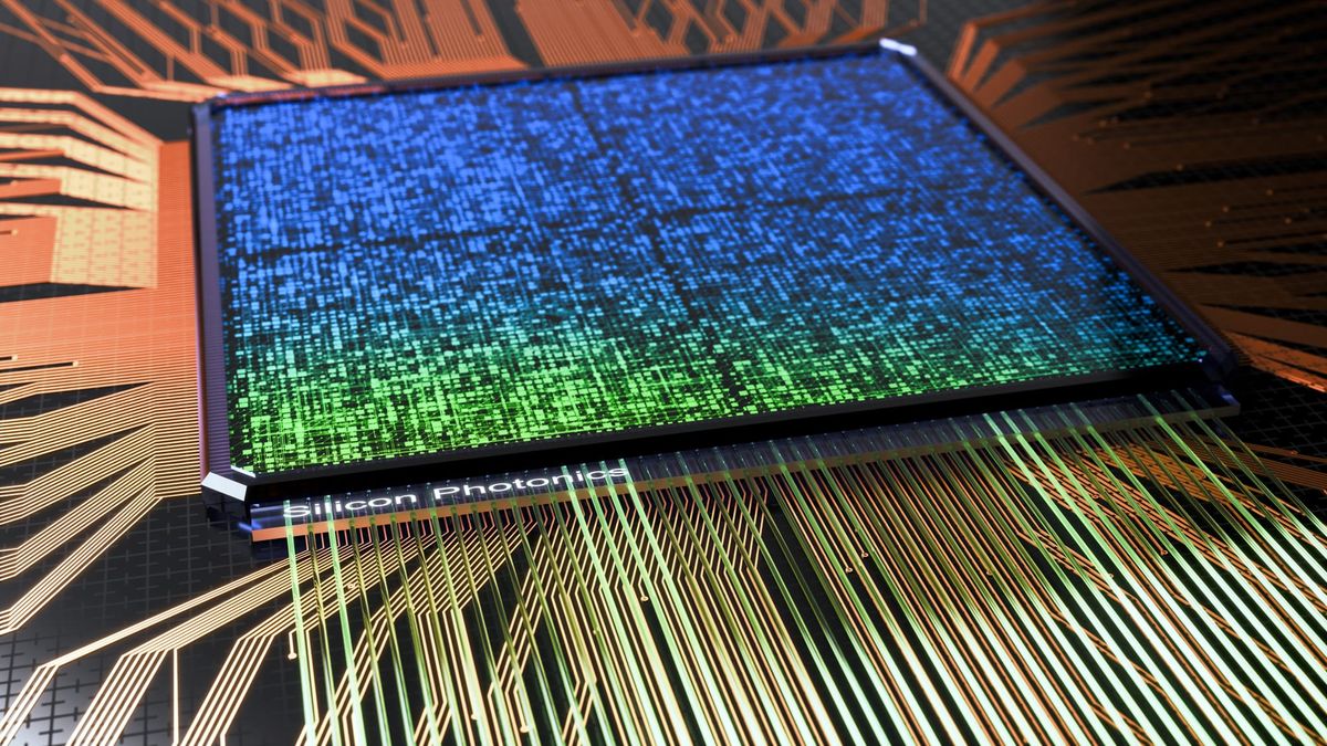
Near-memory and disaggregation photonics keeps data electronic but uses optics to move memory closer to compute in bandwidth and latency terms, and it is where the technology is deployable now. Celestial AI's Photonic Fabric is explicitly a memory-and-compute disaggregation platform (presented at OFC 2025) that pools memory optically so that capacity can scale independently of the GPU's local memory ratio; its acquisition by Marvell is the clearest market validation that this path has near-term revenue potential. Co-packaged optics and optical I/O chiplets (Ayar Labs, Lightmatter Passage, and the incumbent programs at Nvidia, Broadcom, Marvell and Intel) shorten the electrical path and raise bandwidth density without ever storing a bit in the optical domain. Because nothing is stored or computed optically, these systems avoid the endurance, drift and precision problems of Sections 4.3 and 4.4, and they inherit the mature reliability of electronic DRAM while attacking the exact bottleneck (data movement) that the memory wall creates.
4.6 The cross-cutting barrier: conversion overhead
Conversion overhead is the single issue that most often erases photonic advantage. In detailed electro-photonic system models, the data converters and optical interfaces, not the optical compute, dominate energy and area: one 2026 photonic-electronic GEMM system attributed 36 percent of area and 31 percent of power to DACs, roughly 20 percent of area and 19 percent of power to ADCs, and about 12 percent of power to the laser, leaving the photonic multiply path as a small fraction of the budget. Laser power grows exponentially with the optical depth of a tile because insertion loss compounds, so it dominates at large array sizes. A single 8-bit converter pair at several gigasamples per second dissipates tens of femtojoules per sample, and in full-system LLM-inference models the cross-domain conversion plus DRAM traffic routinely exceeds the photonic compute energy. Cutting converter resolution to save energy backfires on accuracy: dropping from 8-bit to 4-bit ADCs has been shown to cost more than 20 percent model accuracy on transformer benchmarks. The takeaway is that any "attojoule-per-MAC" or large-multiplier efficiency claim that quotes only the optical multiply path is a device-level figure and should be discounted; the honest figures are system-level and much closer to parity with electronics.
5. Economic and Market Dynamics
The revenue is in interconnect, and the market data are consistent on this point. A China Insights Consultancy analysis drawing on LightCounting data, prepared for the Yuanjie Semiconductor IPO filing, projects the data-center optical-interconnect market growing from $13.7 billion in 2024 to $144.4 billion by 2030, with silicon photonics rising to roughly 64 percent of revenue; independent CPO-specific forecasts are more modest and more divergent (LightCounting around $10 billion by 2030, Coherent citing $15 billion, and Yole projecting CPO-driven photonics packaging near $5 billion by 2031), which itself signals an early, fast-moving market where estimates are unsettled. Against this, there is no comparable independent market for photonic memory or true in-memory photonic compute; those remain R&D lines and venture bets, not sized markets. The economics of the memory wall favor the interconnect path directly: HBM is sold out through 2026, the HBM market is projected to grow toward $100 billion by 2028, and the value of disaggregation is precisely that it lets operators buy memory capacity and bandwidth without buying proportional compute, which is why hyperscalers and Marvell are paying for it.
Value in the stack is accruing to three layers: the optical-component and laser suppliers (Coherent, Lumentum, now capitalized by Nvidia), the optical-I/O and fabric IP owners (Ayar Labs, Celestial AI inside Marvell, Lightmatter), and the advanced-packaging and foundry base (TSMC, GlobalFoundries, Tower, Intel Foundry, and OSATs such as Amkor and ASE). Capital intensity is high and rising: these are chip-scale products requiring foundry tape-outs, heterogeneous integration and test capacity, which is why even well-funded startups partner with GlobalFoundries or Intel Foundry rather than build fabs, and why the strategic-investor syndicates are dominated by the very GPU and memory incumbents whose roadmaps create the demand. Photonic-compute company projections (Q.ANT's 30x energy and 50x performance claims, Lightmatter's and Celestial's bandwidth-multiplier claims) should be read as company claims pending independent, workload-level verification, and separated from the independent market forecasts above.
6. Risks
The most important risk to a photonics-compute thesis is that electronic alternatives improve faster than photonics can close its system-level gap. Likelihood is high and impact is high: HBM4, processing-in-memory DRAM and analog compute-in-memory macros are advancing on well-capitalized roadmaps, and the system-level efficiency of even the best photonic compute (Lightmatter 2025) is near parity rather than decisively ahead. The credible mitigation is to underwrite photonic compute only where it wins on latency or bandwidth density rather than raw efficiency, and to treat it as a venture option, not a core allocation.
Conversion overhead erasing claimed gains is a near-certainty at the device-claim level and is already visible in system models where converters and lasers dominate energy and area. Its impact is to compress or eliminate the efficiency advantage. Mitigation lies in architectures that amortize conversion through weight reuse, wavelength multiplexing and reduced conversion frequency, and in emerging PCM-based converters; investors should consider system-level, conversion-inclusive numbers before crediting any efficiency claim.
Materials endurance, drift and reliability are the binding risks for nonvolatile photonic memory and true in-memory photonic compute. Likelihood is high and impact is high for those specific paths: cycling endurance on-chip is often only thousands of cycles, multilevel drift corrupts stored weights within seconds to minutes, and write energies are large. Mitigations (encapsulation, nanostructuring, ferroelectric alternatives) are progressing but not yet at the 10^9-plus endurance and stable multilevel retention that a production weight-memory needs. This risk largely does not touch the interconnect path, which is one more reason interconnect is the safer allocation.
Packaging and yield risk is moderate in likelihood and high in impact across all photonic paths, because heterogeneous integration of lasers, modulators and detectors with CMOS is the hardest and least mature manufacturing step; the mitigation is the incumbents' heavy investment in hybrid bonding and OSAT partnerships, which is precisely where capital is flowing. Finally, hype-cycle funding risk is real: valuations in the low-single-digit to mid-single-digit billions for pre-revenue or early-revenue companies (Ayar Labs at $3.75 billion, Lightmatter at $4.4 billion, Celestial at a $3.25 billion-plus deal value with revenue milestones stretching to fiscal 2029) price in execution that has not yet occurred. The mitigation is to favor names with signed hyperscaler engagements, foundry qualification and, ideally, acquisition by a cash-generative incumbent.
 John D
7. Implications for the Technically Informed Investor
The segment that is investable now is optical interconnect and its supply chain, because it has revenue visibility, incumbent validation and a market forecast in the tens of billions, and because it sidesteps the endurance, drift and precision problems that gate the storage and compute paths. Concretely, the most defensible exposure is through the publicly traded optical-component and laser suppliers that the incumbents are capitalizing (Coherent and Lumentum, each backed by a $2 billion Nvidia commitment), and through the diversified semiconductor names that now own or build the fabric and packaging (Marvell, which absorbed Celestial AI; Broadcom and Intel in CPO; and the foundry and memory base of TSMC, GlobalFoundries, SK hynix, Samsung and Micron). Private optical-I/O leaders (Ayar Labs, Lightmatter) offer higher-beta exposure to the same thesis, appropriate for venture allocations with the understanding that their valuations already discount successful high-volume execution.
True in-memory photonic computing is a research-stage option worth tracking but not yet underwriting as a core position. Lightmatter's 2025 result is the milestone that changes the conversation, and its significance is that it reported system-level energy and near-electronic accuracy rather than a device-level multiply figure. Reservoir computing and optical data storage remain research-stage and are not investable on this horizon.
Reasoning forward from current evidence, and labeling this as inference, the milestones that would change the view are specific and measurable. For photonic compute to warrant a core allocation, expect an independent, conversion-inclusive system-level efficiency clearly beyond the best electronic accelerators (a multiple, not parity) on a production workload, sustained at multi-gigahertz clocks. For nonvolatile photonic memory to become an in-memory-compute substrate, expect on-chip endurance above roughly 10^9 cycles with stable multilevel retention (no measurable drift-induced level overlap over operational timescales) and write energies falling into the picojoule range. For the interconnect thesis, the signals to watch are hyperscaler design wins converting to volume shipments, foundry qualification at GlobalFoundries and Intel Foundry, the pace of the copper-to-optics transition inside the rack, and whether Celestial's earnout revenue milestones (a $500 million cumulative threshold and a $2 billion upside case by Marvell's fiscal 2029) are met, which would confirm that memory disaggregation is a real product line and not a defensive acquisition. A stall in any of these, or a surprise step-change in HBM bandwidth or PIM-DRAM economics, would argue for trimming photonic exposure back toward the component and foundry layer.
 Technical Paper Link

References
[1] Fang, Z., et al. 2023. "Electrical Programmable Multilevel Nonvolatile Photonic Random-Access Memory." Light: Science & Applications 12.
[2] Zhang, H., et al. 2023. "Seven Bit Nonvolatile Electrically Programmable Photonics Based on Phase-Change Materials for Image Recognition." ACS Photonics.
[3] Ríos, C., et al. 2015. "Integrated All-Photonic Non-Volatile Multi-Level Memory." Nature Photonics 9: 725–732.
[4] Wuttig, M., H. Bhaskaran, and T. Taubner. 2017. "Phase-Change Materials for Non-Volatile Photonic Applications." Nature Photonics 11: 465–476.
[5] Prabhathan, P., et al. 2023. "Roadmap for Phase Change Materials in Photonics and Beyond." iScience 26.
[6] Zhang, W., and E. Ma. 2020. "Unveiling the Structural Origin to Control Resistance Drift in Phase-Change Memory Materials." Materials Today 41: 156–176.
[7] Dutta, S., et al. 2026. "Increased Endurance of Nonvolatile Photonics Enabled by Nanostructured Phase-Change Materials." Advanced Materials.
[8] Feldmann, J., et al. 2021. "Parallel Convolutional Processing Using an Integrated Photonic Tensor Core." Nature 589: 52–58.
[9] Ahmed, S. R., et al. 2025. "Universal Photonic Artificial Intelligence Acceleration." Nature 640: 368–374.
[10] Zhang, Z., et al. 2025. "Multimode-Enabled Silicon Photonic Delay Lines: Break the Delay-Density Limit." Light: Science & Applications 14.
[11] Petrini, M., et al. 2023. "Variable Optical True-Time Delay Line Breaking Bandwidth-Delay Constraints." Optics Letters 48 (2): 460.
[12] Vandoorne, K., et al. 2014. "Experimental Demonstration of Reservoir Computing on a Silicon Photonics Chip." Nature Communications 5.
[13] Estébanez, I., A. Argyris, and I. Fischer. 2023. "Experimental Demonstration of Bandwidth Enhancement in Photonic Time Delay Reservoir Computing." Optics Letters 48 (9): 2449–2452.
[14] Grimaldi, V., et al. 2026. "High-Speed Non-Volatile Barium Titanate Field-Programmable Photonic Gate Array." Nature Photonics.
[15] Demirkiran, C., et al. 2023. "An Electro-Photonic System for Accelerating Deep Neural Networks." ACM Journal on Emerging Technologies in Computing Systems 19 (4).
[16] Marvell Technology, Inc. 2026. Form 10-K, FY2026, and Form 10-Q filings. U.S. Securities and Exchange Commission.
[17] Sahni, S., et al. 2025. "Photonic Fabric for Memory and Compute Disaggregation." Optical Fiber Communication Conference (OFC) 2025, paper W3D.1.
[18] Ríos, C., et al. 2019. "In-Memory Computing on a Photonic Platform." Science Advances 5: eaau5759.
[19] China Insights Consultancy / LightCounting. 2024. Data Center Optical Interconnect Market Forecast (Yuanjie Semiconductor IPO filing).
[20] Coherent Corp. 2026. Form 8-K, March 2, 2026. U.S. Securities and Exchange Commission.
[21] Ayar Labs. 2026. "Ayar Labs Raises $500 Million Series E." Company announcement, March 3, 2026.
[22] NVIDIA Corporation. 2026. "NVIDIA and Coherent / NVIDIA and Lumentum Strategic Partnership Announcements." March 2, 2026.