The Silicon Photonics Supply Chain: SOITEC, Fabrinet, and the Photoresist Bottlenecks Behind Optical Interconnect
One French firm makes 90%+ of photonics-grade SOI; Japan makes 91% of photoresist. Mapping the bottlenecks behind optical computing.

Photoresist, SOI, and Silicon Photonics: Inside the Optical Interconnect Supply Chain Powering Data Centers
1. Summary
1.1 Principal judgment
The supply chain for photoresist silicon wafers is in fact three distinct, interlocking industries: photoresists (light-sensitive specialty chemicals), engineered silicon substrates (including silicon-on-insulator and photonics-grade SOI), and silicon-photonics manufacturing and packaging. SOITEC (Euronext Paris: SOI) sits in the second domain as the dominant supplier of photonics-grade SOI; Fabrinet (NYSE: FN) sits in the third as the leading independent optical and photonic contract manufacturer. The photoresist layer is upstream of both, supplied by a small group of mostly Japanese chemical firms. The central finding of this report is that the AI-driven build-out of data-center optical interconnect has converted what were once cyclical specialty markets into strategic bottlenecks, and that the most acute concentration risks lie not in the multi-billion-dollar wafer or photoresist markets in aggregate but in narrow, high-specification niches: photonics-grade SOI (where SOITEC holds greater than 90% share), EUV photoresist (where four Japanese firms hold roughly 75%), and advanced optical packaging (where Fabrinet is the sole or primary outsourced partner for the largest AI customers) [1][11][9].
1.2 Most consequential quantified findings
SOITEC reported fiscal-year 2025 (ended March 31, 2025) revenue of 891 million euros, down 9% year on year from 978 million euros in fiscal 2024, with an EBITDA margin of 33.5%; the company described POI as its "fourth product to generate annual revenue of around $100m or more," and Photonics-SOI revenue crossed 100 million dollars in fiscal 2026, earlier than the company had anticipated [1][3]. Fabrinet reported record fiscal-year 2025 (ended June 27, 2025) revenue of 3.42 billion dollars, up 18.6%; its two largest customers, NVIDIA and Cisco Systems, contributed 27.6% and 18.2% of revenues respectively (45.8% combined), with NVIDIA's portion having declined from 35.1% in fiscal 2024 [4]. The silicon-photonics device market is estimated at between 1.8 and 3.27 billion dollars in 2025 depending on the source, with consensus forecasts converging on roughly 9 to 10 billion dollars by 2030 [11][12][13][15]. The global photoresist market is estimated at roughly 2.9 to 5.5 billion dollars in 2024-2025 depending on segmentation [8][9]. JSR Corporation, the world's largest photoresist maker at roughly 27% share, was taken private by the Japan Investment Corporation in a deal valued at roughly 909 billion yen (about 6.4 billion dollars), delisting from the Tokyo Stock Exchange on June 25, 2024 [18][19].
1.3 Key risks
The dominant systemic risks are geographic and single-supplier concentration. Japanese producers account for roughly 91% of the global photoresist market; a single French firm dominates photonics-grade SOI; Taiwan dominates leading-edge fabrication; and a single Thailand-based contract manufacturer dominates advanced optical packaging for the largest AI customers [19][9][4]. These bottlenecks are individually small in dollar terms but systemically critical: a disruption at any one would propagate through the entire AI-infrastructure build-out. Export-control escalation between the United States, its allies, and China, plus environmental regulation of PFAS chemistries in photoresists, are the two regulatory vectors most likely to reshape the landscape over the next 24 to 36 months [24][32].
1.4 Central recommendations
Investors should treat SOITEC and Fabrinet as differentiated, high-quality but concentration-exposed plays on optical interconnect, sizing positions to reflect single-customer and single-product dependencies. Defense and industrial-policy analysts should map and stress-test the photonics-grade SOI and EUV-photoresist bottlenecks with the same rigor applied to leading-edge logic and high-bandwidth memory, since these materials are dual-use and currently lack redundant qualified suppliers. Procurement leaders should pursue dual-sourcing and strategic inventory for photoresist and engineered substrates wherever qualification timelines permit, recognizing that qualification cycles of multiple years are themselves the binding constraint.
The Photoresist, Engineered-Substrate, and Silicon-Photonics Ecosystem: A Strategic Intelligence Assessment of SOITEC, Fabrinet, and the Supply Chain Behind Optical Computing
2. Contextual Background
2.1 The three domains disambiguated
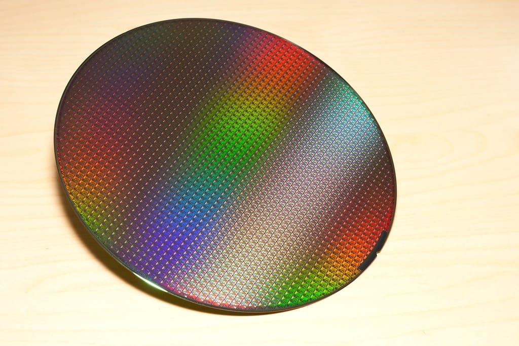
The phrase "photoresist silicon wafers" conflates three separate links in the semiconductor and photonics value chain. The first is photoresists: light-sensitive polymer or metal-oxide formulations applied to a wafer surface, exposed through a photomask, and developed to create the patterns that define circuit features. Photoresists are a specialty-chemicals business measured in billions of dollars and dominated by Japanese suppliers [8][9]. The second is silicon wafers and engineered substrates: the physical disks of crystalline silicon (bare polished, epitaxial, or engineered) on which devices are built. Engineered substrates such as silicon-on-insulator (SOI) add a buried oxide layer that confers electrical or optical advantages. The third is silicon-photonics manufacturing and packaging: the fabrication of photonic integrated circuits (PICs) and their assembly into optical modules and co-packaged optics, where specialized foundries and contract manufacturers operate.
These domains are sequential and interdependent: photoresist is consumed during fabrication on substrates that may be engineered, and the resulting photonic devices are then packaged and tested. SOITEC is in the engineered-substrate domain and Fabrinet is in the photonics-manufacturing-and-packaging domain, with the photoresist layer upstream of both.
2.2 Photolithography and the role of photoresist
Photolithography is the central patterning step of semiconductor manufacturing. A photoresist is spin-coated onto the wafer, soft-baked, exposed to ultraviolet light through a mask, and developed; the remaining resist protects selected regions during etching or deposition [21]. The resolution achievable depends on the exposure wavelength and the resist chemistry. The industry has progressed from i-line (365 nm) and KrF (248 nm) through ArF (193 nm) immersion to extreme ultraviolet (EUV, 13.5 nm). Each transition has demanded new resist chemistries: at sub-5 nm logic nodes, photon shot noise and line-edge roughness threaten yield, driving a shift toward metal-oxide and hybrid organic-inorganic EUV resists [9].
The qualification of a new resist for a given process can take many months of work, which is the structural reason the supplier base is small and switching is slow [21]. In photonics, photoresist patterns the waveguides, modulators, and grating couplers of a PIC; while photonic features are generally larger than leading-edge logic features, the resist must still deliver tight dimensional control because waveguide geometry determines optical loss. The interaction of photoresist with both the substrate and the photonics domains makes it a cross-cutting dependency rather than a parallel one.
2.3 The emergence of silicon photonics
Silicon photonics uses CMOS-compatible processes to build optical components (waveguides, modulators, photodetectors) on silicon, allowing data to move as light rather than electrons. The technology matured slowly: industry analysts note it took roughly a decade after early commercialization to make a big impact on the optical-transceiver market, and decisions by large companies including Cisco, Huawei, and Intel helped accelerate adoption [35]. The catalyst for the current inflection has been artificial intelligence. AI training and inference require enormous bandwidth between GPUs, and copper interconnect runs out of reach and energy efficiency at the data rates (800 Gb/s, 1.6 Tb/s) AI clusters now demand.
The energy dimension is acute. According to the U.S. Department of Energy and Lawrence Berkeley National Laboratory's "2024 Report on U.S. Data Center Energy Use" (December 20, 2024), data centers consumed about 4.4% of total U.S. electricity in 2023 (about 176 terawatt-hours) and are expected to consume between 6.7% and 12% of total U.S. electricity by 2028, rising to between 325 and 580 terawatt-hours [13]. This intensifies the search for energy-efficient optical interconnect. Silicon photonics, and specifically co-packaged optics, is the industry's principal answer.
2.4 Engineered substrates and SOI
A silicon-on-insulator wafer is, in effect, a silicon sandwich: a thin crystalline silicon device layer on top, a buried oxide (BOX) insulating layer in the middle, and a thick silicon handle wafer below for mechanical support. The BOX reduces parasitic capacitance, improving speed and power efficiency, and isolates devices from the substrate. Different applications require different layer stacks: RF-SOI for smartphone radio-frequency front ends; FD-SOI (fully depleted SOI) for low-power logic; Power-SOI for automotive; and Photonics-SOI for optical waveguides.
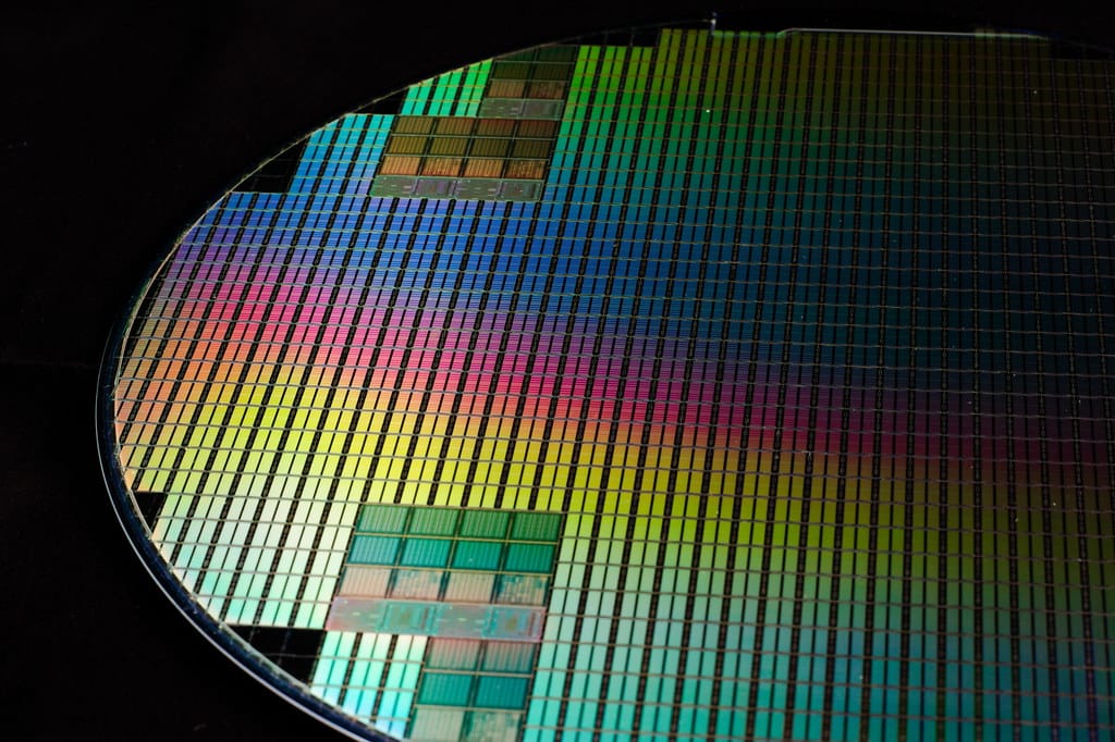
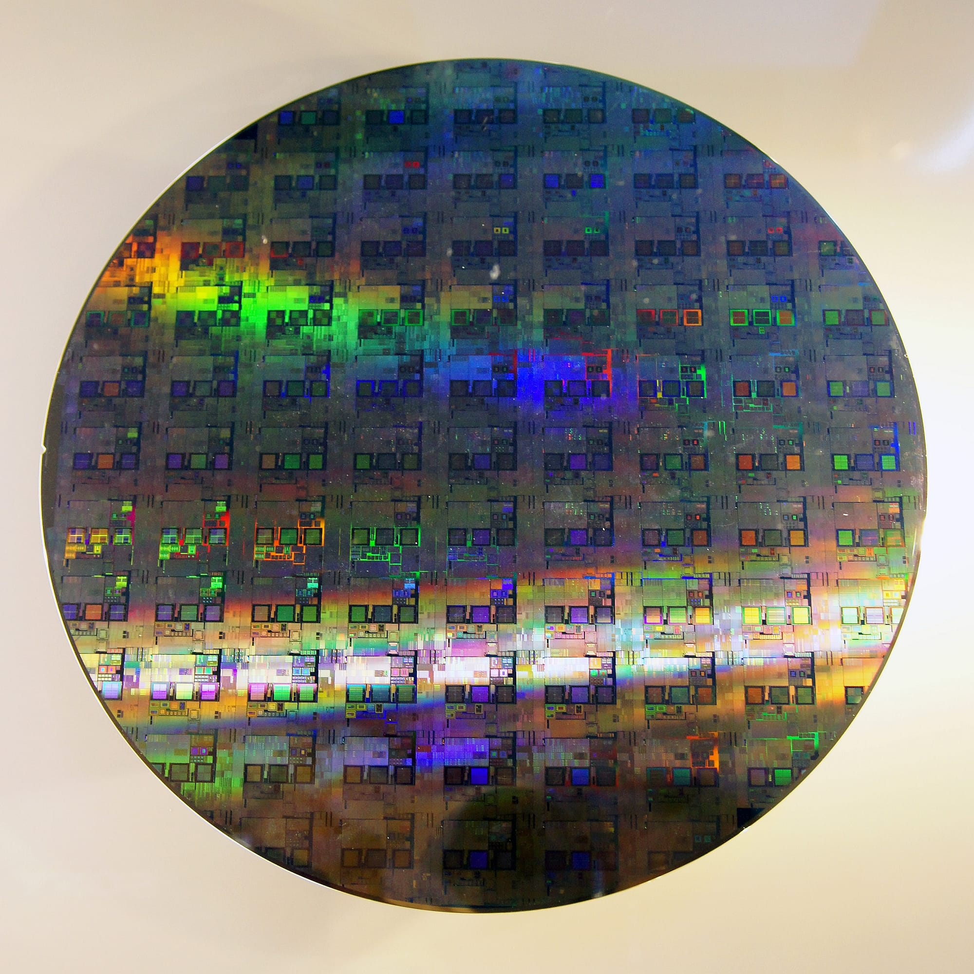
Photonics-grade SOI is the most demanding variant. SOITEC engineers it to a roughly 220 nm top silicon layer on a buried oxide of approximately 1 to 3 microns, with silicon-thickness uniformity reportedly within about 1 nm across the wafer and very low defect density, because the BOX thickness determines how well light is confined and any deviation adds optical loss to every waveguide on the chip [38]. This precision is the basis of SOITEC's competitive moat; the specifications must be individually qualified with each foundry, which is why a multi-supplier SOI market in aggregate coexists with an effectively single-sourced photonics-grade niche.
2.5 Why this supply chain matters strategically
These three domains underpin computation, data-center interconnect, telecommunications, sensing (including automotive LiDAR), and defense systems. The strategic significance flows from concentration: each domain has a narrow apex where one country or one company is effectively irreplaceable in the near term. Photoresist is concentrated in Japan; photonics-grade SOI in France; leading-edge fabrication and advanced packaging in Taiwan; and advanced optical assembly in Thailand [19][38][4]. Because AI infrastructure is now a matter of national economic and military competitiveness, these once-obscure materials and services have become objects of industrial policy and export control. The remainder of this report maps the players, the technology, the economics, the regulation, and the geopolitics, and derives recommendations tailored to distinct audiences.
3. Key Players and Stakeholders
3.1 SOITEC: the engineered-substrate apex
SOITEC S.A. (Euronext Paris: SOI; US OTC: SLOIF/SLOIY), founded in 1992 and headquartered in Bernin, near Grenoble in the French Alps, is the global leader in SOI and related engineered substrates [1]. Its core process technology, Smart Cut, transfers an ultra-thin layer of silicon from a donor wafer onto an oxidized handle wafer using hydrogen-ion implantation and thermal cleaving; the donor remainder is recycled, which is central to the cost structure [38]. SOITEC's product platforms span RF-SOI and POI (piezoelectric-on-insulator) for mobile communications, FD-SOI for low-power computing, Power-SOI and SmartSiC (silicon carbide) for automotive and industrial, Imager-SOI (being phased out), and Photonics-SOI for optical interconnect [1].
The company reports in three segments. Mobile Communications generated 546 million euros in fiscal 2025 (61% of revenue) and was the principal drag, hit by an RF-SOI inventory correction at customers. Edge and Cloud AI generated 216 million euros, growing on Photonics-SOI and FD-SOI. Automotive and Industrial generated 129 million euros, down on weak Power-SOI demand [1]. Its 300 mm SOI fabs in Bernin and Singapore support tens of thousands of wafers per month [38]. In photonics-grade SOI, SOITEC's position approaches a monopoly; one analyst summary cited a Bank of America estimate of greater than 95% market share, and the company is qualified for volume photonics-grade SOI by Tower Semiconductor, GlobalFoundries, and TSMC [38]. SOITEC's chief executive transitioned during 2025, and the company guided to fiscal-2027 profitability being affected by low fab loading, currency, and lower funding [2].
3.2 Fabrinet: the optical-packaging apex
Fabrinet (NYSE: FN), headquartered in the Cayman Islands with primary operations in Thailand, is the leading independent provider of advanced optical packaging and precision optical, electro-mechanical, and electronic contract manufacturing [4]. It reported record fiscal-2025 revenue of 3.42 billion dollars, up 18.6% from 2.88 billion dollars in fiscal 2024, with optical-communications products at 76.6% of revenue and automotive, industrial lasers, and other markets at 23.4% [4]. The company's defining characteristic is customer concentration: NVIDIA and Cisco Systems contributed 27.6% and 18.2% of fiscal-2025 revenues respectively, together accounting for 45.8%; NVIDIA's share had declined from 35.1% in fiscal 2024, reflecting both Cisco's growth and a broadening base [4]
Fabrinet is a named member of NVIDIA's silicon-photonics co-packaged-optics ecosystem and is, in many cases, the sole outsourced manufacturing partner used by its customers for the products it makes [4][34]. Its role spans the assembly and test of optical transceivers (including 800G and 1.6T modules), reconfigurable optical add-drop multiplexers, and the precision packaging that co-packaged optics requires. Quarterly revenue continued to accelerate, reaching 1.214 billion dollars for the quarter ending March 2026, up roughly 39% year on year [7]. The company has also run a substantial share-repurchase program, signaling management confidence in sustained demand [6].
3.3 Photoresist suppliers
The photoresist market is highly concentrated among Japanese firms. JSR Corporation, the world's largest at roughly 27% share according to Nomura Securities, was acquired by the state-backed Japan Investment Corporation (JIC) and delisted from the Tokyo Stock Exchange on June 25, 2024; the deal valued JSR at roughly 909 billion yen (about 6.4 billion dollars) [18][19]. JSR's EUV resist capability is anchored by its 2021 acquisition of Oregon-based Inpria, a metal-oxide resist specialist, and it settled long-running patent litigation with Lam Research into a cross-licensing agreement covering dry-resist EUV patterning in 2024 [19]. Tokyo Ohka Kogyo (TOK; Tokyo: 4186) is a close competitor and has a development agreement with Intel for sub-2 nm resists [9].
Shin-Etsu Chemical (Tokyo: 4063), Sumitomo Chemical (Tokyo: 4005), and Fujifilm (Tokyo: 4901) round out the leading Japanese suppliers; together, Japanese producers account for roughly 91% of the global market according to Nikkei reporting, and TOK, JSR, Shin-Etsu, and Fujifilm hold roughly 75% of the EUV resist segment specifically [19][9]. Western suppliers include Merck KGaA (Frankfurt: MRK; through AZ Electronic Materials) and DuPont (NYSE: DD) [8]. South Korea's Dongjin Semichem began supplying EUV photoresist to Samsung Foundry's 3 nm lines in 2025 [9]. Chinese entrants such as Hubei Dinglong, Xuzhou B&C Chemical (backed by Huawei's Hubble Investment arm), Jiangsu Nata, and Shanghai Sinyang are emerging but lag on defect density [19].
3.4 Wafer and substrate producers
The bare silicon wafer market is an oligopoly: Shin-Etsu Chemical, SUMCO (Tokyo: 3436), GlobalWafers (Taipei: 6488), Siltronic (Frankfurt: WAF), and SK Siltron (a subsidiary of SK Group) together hold roughly 82% of revenue, with 300 mm wafers representing about 75% of value [17]. GlobalWafers' attempted acquisition of Siltronic and its CHIPS-funded Texas plant are notable consolidation and reshoring moves [17]. In SOI specifically, SOITEC dominates; Shin-Etsu holds a Smart Cut royalty license but sells little photonics-grade volume; GlobalWafers' Smart Cut license was terminated in 2023 with a settlement extending its market participation only to 2027; and China's NSIG/Simgui produces 200 mm SOI largely for the domestic market, with output contractually distributed by SOITEC worldwide [38]. Estimates of SOITEC's overall SOI share cluster around 70%, with greater than 90% in FD-SOI and photonics-grade SOI [38].

3.5 Photonics foundries and module integrators
The silicon-photonics foundry landscape is narrow. GlobalFoundries (Nasdaq: GFS) offers its Fotonix platform (built on its 45 nm SOI heritage) and in 2025 acquired Singapore's Advanced Micro Foundry (AMF) to become, by its own description, the world's largest pure-play silicon-photonics foundry, targeting more than 1 billion dollars in annual photonics revenue by the end of the decade [35]. Tower Semiconductor (Nasdaq: TSEM) offers the PH18 platform (180 nm, 200 mm) and a newer 300 mm process, with active variants integrating InP and GaAs lasers [36]. TSMC (NYSE: TSM; TWSE: 2330) is developing co-packaged-optics and integrated-photonics capability tied to its advanced packaging [34]. Intel (Nasdaq: INTC) has long-standing silicon-photonics activity.
Downstream module integrators and component suppliers include Lumentum (Nasdaq: LITE), Coherent (NYSE: COHR), Cisco (Nasdaq: CSCO, including its Acacia coherent-DSP and silicon-photonics operations), Broadcom (Nasdaq: AVGO), and Marvell (Nasdaq: MRVL) [11][39]. Coherent, formed from II-VI's acquisition of the former Coherent, reported quarterly revenue of 1.43 billion dollars in its fiscal second quarter of 2025 (up 27% year on year) and has begun shipping 1.6T datacom transceivers and a liquid-crystal optical circuit switch [39]. ASML (Nasdaq/Euronext: ASML) is the monopoly supplier of EUV lithography systems and thus a critical enabler upstream of the resist and patterning layer [20].
3.6 Governments and standards bodies
Governments are now central actors through subsidy and export-control regimes: the United States (CHIPS and Science Act, Bureau of Industry and Security export controls), the EU (European Chips Act), Japan (METI, NEDO, JIC, and the Rapidus initiative), Taiwan (Statute for Industrial Innovation), South Korea (K-Chips Act), and China (national IC investment funds) [24][27][30][43][41]. Standards and research bodies include SEMI (industry standards and market data), imec (Belgium's research institute, central to EUV-resist and photonics R&D), CEA-Leti (France, SOITEC's research partner), AIM Photonics (United States), and the Wassenaar Arrangement (multilateral export-control coordination among 42 states) [28][22].
4. Technical and Operational Considerations
4.1 Substrate engineering and the Smart Cut moat
SOITEC's Smart Cut process is the operational heart of the engineered-substrate domain. A donor wafer is oxidized to grow the buried oxide layer (BOX), implanted with hydrogen ions to create a weakened cleave plane, bonded to a handle wafer, and thermally split; the thin transferred layer becomes the device silicon, and the donor remainder is re-polished and reused [38]. The process can control top-silicon thickness to a few angstroms; SOITEC cites uniformity of roughly 3.2 angstroms for ultra-thin SOI [38]. For photonics, the BOX must be thick enough (1 to 3 microns) to prevent the optical mode's evanescent tail from leaking into the handle wafer, and the top silicon must be uniform to roughly 1 nm [38].
These specifications must be individually qualified with each foundry, and the multi-year qualification cycle is the principal barrier to a second source. This is why, despite a multi-supplier SOI market in aggregate, photonics-grade SOI is effectively single-sourced today. The economic elegance of donor recycling, combined with decades of accumulated process knowledge and intellectual property, entrenches the incumbent. Evidence suggests a second supplier could eventually be qualified, but the relevant question is whether that takes two years or five, and whether SOITEC uses the interval to extend its lead.
4.2 Photoresist chemistry and resolution limits
Resist performance is governed by the resolution-line-edge-roughness-sensitivity trade-off (the "RLS triangle"): improving one typically worsens another. As features shrink, chemically amplified resists used at 193 nm and 248 nm give way at EUV to metal-oxide resists (such as those from JSR's Inpria) that offer higher absorption and etch resistance [9]. High-NA EUV introduces higher-aspect-ratio patterning and new soak conditions that require fresh resist validation, prompting suppliers such as JSR, Fujifilm, and Shin-Etsu to validate resist performance under new conditions [9]. The industry is also pursuing dry-resist deposition, an area where the JSR/Inpria and Lam Research cross-licensing arrangement is significant [19].
For photonics and advanced packaging, a distinct and growing sub-segment uses thick negative-tone and epoxy-based resists for fan-out wafer-level packaging and deep features [9]. The chemistry requirements differ markedly from leading-edge logic resists, which is why the supplier ecosystem, while concentrated, is also segmented by application. The persistent constraint across all segments is the months-to-years qualification timeline, which makes the resist layer slow to diversify even when alternative chemistries exist.
4.3 Lithography nodes and their relevance to photonics
Photonic features are generally coarser than leading-edge logic, so silicon photonics is typically manufactured on mature nodes (180 nm at Tower's PH18, 45 nm and similar at GlobalFoundries Fotonix) rather than at the EUV frontier [36][35]. This decoupling matters strategically: the photonics bottleneck is not EUV lithography or leading-edge logic capacity but the engineered substrate (photonics-grade SOI), the integration of III-V lasers (InP, GaAs) onto silicon, and the packaging [38][36]. The relevant bottlenecks therefore differ from those in leading-edge logic, and policy attention calibrated only to EUV and sub-3 nm logic will miss the photonics-specific dependencies. This is a recurring analytical error in coverage that treats "semiconductors" as a monolith.
4.4 Wafer-scale integration, packaging, and co-packaged optics
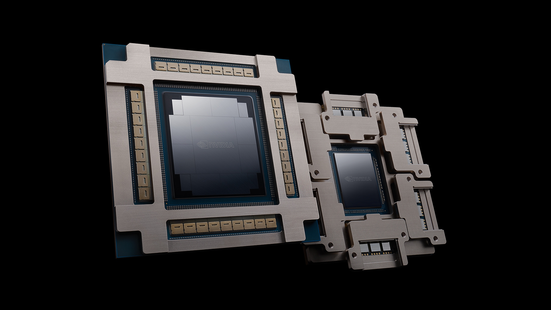
Co-packaged optics (CPO) is the most consequential architectural shift in the ecosystem. Conventional pluggable transceivers convert electrical to optical signals at the faceplate, incurring electrical loss across the board and connectors and requiring digital signal processors that consume significant power (a 1.6 Tbps transceiver may use around 30 watts, with the DSP consuming more than half) [34][40]. CPO places the optical engine directly beside the switch ASIC on the same package, eliminating the long electrical path. NVIDIA's Spectrum-X and Quantum-X Photonics switches, unveiled on March 18, 2025, "integrate optics innovations with 4x fewer lasers to deliver 3.5x more power efficiency, 63x greater signal integrity, 10x better network resiliency at scale and 1.3x faster deployment," with the Spectrum SN6800 delivering 409.6 Tb/s across 512 ports at 800 Gb/s [34].
NVIDIA's photonics ecosystem explicitly names TSMC, Browave, Coherent, Corning, Fabrinet, Foxconn, Lumentum, SENKO, SPIL, Sumitomo Electric Industries, and TFC Communication [34]. Broadcom's competing Tomahawk-Davisson CPO line, developed with Meta, recorded over a million cumulative device-hours of flap-free operation in testing, an early but significant reliability signal [40]. CPO fundamentally shifts packaging value from module assembly toward on-board photonic die integration, flip-chip, and wafer-level packaging, which benefits foundries (for the photonic die) and advanced packagers such as Fabrinet (for the integration) [40][4].
4.5 Yield, process maturity, and operational dependencies
Silicon-photonics yield and average selling price have historically been weaker than electronics, and analysts have repeatedly revised photonics device forecasts downward to reflect this [37]. Laser integration (attaching or bonding III-V material to silicon) remains the hardest manufacturing step and a key differentiator among foundries; Tower's active PH18 variants integrate InP and GaAs lasers, while GlobalFoundries enables laser attachment via cavities chiseled into the die [36][35]. Operationally, the ecosystem has cascading single points: photonics-grade SOI from SOITEC feeds the foundries (Tower, GlobalFoundries, TSMC), whose photonic die feed packagers and integrators (Fabrinet, OSATs), whose modules feed the switch and GPU makers (NVIDIA, Broadcom) [38][4][34]. A disruption at the SOITEC or Fabrinet layer would propagate forward with limited near-term substitution.
4.6 Photoresist as a cross-cutting dependency
Photoresist interacts with both other domains. In the substrate domain, resist is consumed when foundries pattern devices on SOI; in the photonics domain, resist patterns the waveguides and couplers. Because photoresist has a limited shelf life, stockpiling offers only a partial and temporary buffer against supply disruption, as the 2019 Japan-Korea episode demonstrated, when Korean firms accumulated months of inventory but could not eliminate dependence [21]. The combination of limited shelf life, multi-year qualification cycles, and geographic concentration makes photoresist the most structurally fragile cross-cutting input in the ecosystem.
5. Economic and Market Dynamics
5.1 Market sizing and divergence across sources
Market-size estimates diverge materially and should be treated with caution; the divergence is itself an analytical finding. For silicon-photonics devices, 2025 estimates range from 1.8 billion dollars (Global Market Insights) to 2.65 billion dollars (MarketsandMarkets) to 3.11 billion dollars (Mordor Intelligence) to 3.27 billion dollars (Fortune Business Insights), with 2030 forecasts clustering around 9.6 to 10.4 billion dollars and implied CAGRs of 25% to 30% [14][12][11][15]. For photoresists, the Mordor Intelligence estimate is 2.91 billion dollars in 2025, while Global Market Insights cites 5.5 billion dollars in 2024 for "photoresist chemicals for advanced lithography"; these differ because of segmentation (resist only versus resist plus ancillary chemistries) [8][9].
For bare silicon wafers, estimates cluster around 14 to 15 billion dollars in 2024 [16][17]. For SOI wafers specifically, estimates range from roughly 1.3 billion dollars to 1.8 billion dollars in 2024 [38]. The divergence reflects definitional differences (device versus component, resist versus formulation chemistry), and analysts should anchor to the segmentation that matches their question rather than to a single headline number. Where this report cites a range, the range is the honest representation of the state of available data.
5.2 Demand drivers
The dominant demand driver across all three domains is AI and data-center interconnect. The optical-interconnect market is forecast by some analysts to grow from roughly 14 billion dollars to over 70 billion dollars by 2030, a figure SOITEC and Bank of America have cited [38]. Co-packaged optics could become the mainstream switch architecture, with LightCounting and others projecting that linear-drive pluggables and CPO will double silicon-photonics' share of the transceiver market from roughly 30% in 2025 to 60% in 2030 [35]. Secondary drivers include telecom (5G and early 6G), automotive (FD-SOI for microcontrollers and radar; FMCW LiDAR using silicon photonics), and sensing and medical applications [11][1]. RF-SOI for smartphones remains a large but cyclically depressed segment, the principal cause of SOITEC's fiscal-2025 revenue decline [1].
5.3 Pricing, margins, and capital intensity
Engineered substrates command premium pricing: SOI wafers are reported to be 30% to 40% more expensive than bulk silicon. SOITEC's gross margins fell from roughly 37% in 2023 to roughly 32% in fiscal 2025 (and to 16.3% in the first half of fiscal 2026 on low fab loading), illustrating the operating leverage and cyclicality of capital-intensive substrate manufacturing: fabs cost money whether or not they run [2]. Fabrinet, as a contract manufacturer, operates on thinner gross margins but with high asset turns and strong cash generation, posting record EPS through fiscal 2025 [4][6]. Photoresist is high-margin specialty chemistry where the moat is qualification depth and purity rather than price; resist makers spend roughly 8% to 12% of revenue on R&D [8]. All three domains are capital- and R&D-intensive.
5.4 Capacity expansion
Capacity is expanding across the chain. SOITEC is expanding its Bernin and Singapore 300 mm capacity [38]. Japanese resist makers are building capacity near customers: Fujifilm expanded its Kumamoto EUV-resist capacity by 30% in 2025 for TSMC; JSR is building a Taiwan plant near TSMC and a Korean plant slated for 2026; Shin-Etsu is building in Gunma and has opened additional capacity [9][19]. GlobalWafers opened a CHIPS-funded 300 mm plant in Texas, supported by a 406-million-dollar Commerce Department award [17]. These moves reflect both demand growth and a policy-driven push to localize critical-material supply near fabrication.
5.5 Concentration and market share
Concentration is the defining structural feature. In bare wafers, the top five hold roughly 82% [17]. In SOI, SOITEC holds roughly 70% of the overall market and greater than 90% of photonics-grade and FD-SOI [38]. In photoresist, Japanese firms hold roughly 91% overall and the top four hold roughly 75% of EUV [19][9]. In advanced optical packaging, Fabrinet is the primary outsourced partner for the largest AI customers [4]. This concentration is the source of both pricing power and systemic risk; the two are inseparable.
5.6 Merger, acquisition, and investment activity
M&A and strategic investment have been intense. JIC took JSR private in 2024 [18]. GlobalFoundries acquired AMF in 2025 [35]. GlobalWafers pursued Siltronic [17]. Coherent was formed from II-VI's acquisition of the former Coherent and has been streamlining its portfolio toward datacenter and communications growth engines [39]. NVIDIA made roughly 2-billion-dollar equity investments in both Coherent and Lumentum to secure optical-component supply, a striking signal of supply-chain tightness [40]. Nokia moved to acquire Infinera in 2024 for coherent-DSP and laser capability [11]. These moves reflect a race to secure vertically integrated control of the optical-interconnect supply chain.
6. Regulatory Landscape
6.1 US export controls (BIS)
The U.S. Bureau of Industry and Security has issued three major rounds of advanced-semiconductor export controls (October 2022, October 2023, and December 2, 2024) [25][26]. The December 2024 package added controls on 24 types of semiconductor manufacturing equipment and three software tools, new controls on high-bandwidth memory (HBM) via a new ECCN 3A090.c and the Foreign Direct Product Rule, 140 Entity List additions, and a new Footnote 5 designation [24][25]. China retaliated on December 3, 2024, by banning exports of gallium, germanium, and antimony to the United States [25]. These controls bear on the ecosystem because HBM, advanced packaging, and the equipment that uses photoresist are all in scope, and because gallium is critical to the compound-semiconductor lasers used in photonics [25].
6.2 Japan's export controls (2019 and 2023, distinguished)
Two distinct Japanese measures are frequently conflated and must be separated. In July 2019, Japan tightened export licensing to South Korea for three chemicals: fluorinated polyimide, photoresist, and high-purity hydrogen fluoride, requiring individual rather than bulk licenses [21][20]. South Korea imported roughly 92% to 94% of its photoresist from Japan at the time [21]. The episode triggered Korean localization, diversification to Belgian and other suppliers, and a WTO complaint; Japan restored Korea to its trade whitelist in 2023 [20]. Separately, effective July 23, 2023, METI imposed licensing on 23 categories of advanced semiconductor manufacturing equipment under the Foreign Exchange and Foreign Trade Act, applying to all destinations but with simplified procedures for 42 Wassenaar states [22][23]. Japan expanded the list further in 2024 [23]. The crucial distinction: the 2019 measure targeted materials (including photoresist); the 2023 measure targeted equipment.
6.3 US CHIPS Act
The U.S. CHIPS and Science Act provided 52.7 billion dollars for semiconductor manufacturing, research, and workforce development, plus a 25% investment tax credit [29]. It has catalyzed major fabs (TSMC Arizona, Intel, Micron) and material projects (GlobalWafers' 406-million-dollar award for Texas wafer capacity) [17][29]. The Act funds substrate and materials localization directly relevant to this ecosystem, and it is augmented by state incentives such as New York's 5.5-billion-dollar package for Micron [29].
6.4 European Chips Act
The European Chips Act (Regulation 2023/1781, in force September 2023) aims to mobilize at least 43 billion euros in policy-driven public investment, matched by private investment, and to double the EU's global chip share to 20% by 2030 [27][28]. The European Court of Auditors and others have judged the headline targets unlikely to be met on schedule; only about 4.5 billion euros is directly EU-controlled, with the remainder dependent on member-state state aid [28]. Intel's July 2025 cancellation of its roughly 30-billion-euro Magdeburg fab was a significant setback [28]. SOITEC, as a French substrate champion, and STMicroelectronics (its SmartSiC partner) operate within this policy environment, which also funds an IPCEI initiative explicitly covering photonics and advanced packaging [28].
6.5 Japan (METI, Rapidus), Taiwan, Korea, China
Japan has committed heavily to Rapidus, its 2 nm foundry venture targeting mass production by 2027; total government support has reached roughly 2.35 trillion yen, and a February 2026 round of 268 billion yen included a 100-billion-yen IPA investment and participation by 32 companies, making the government the largest shareholder with an 11.5% voting stake and a golden share [30][31].
Taiwan's Statute for Industrial Innovation (Article 10-2, amended and passed January 7, 2023) grants a 25% tax credit on forward-looking innovative R&D expenditure and a 5% credit on advanced-process equipment, effective through December 31, 2029, for firms holding a key position in the global supply chain; eligibility requires R&D expenses reaching NT$6 billion and an effective tax rate of 12% in 2023 rising to 15% for 2024 to 2029 [43][44]. This is the policy underpinning of Taiwan's so-called silicon shield, given that Taiwan produces over 60% of the world's chips and more than 90% of advanced semiconductors [43][44].
South Korea's K-Chips Act, passed in March 2023, originally raised facility-investment tax credits to 15% for large firms and 25% for SMEs; a February 27, 2025 revision raised these to 20% and 30% respectively and extended semiconductor tax credits to 2031 [41]. Separately, in January 2024 President Yoon announced a Yongin/Gyeonggi semiconductor mega-cluster drawing combined investment of 622 trillion won (about 471 billion dollars) by 2047 [42], and a further 26-trillion-won support package followed in May 2024. A Special Semiconductor Act enabling direct subsidies was progressing through the National Assembly committee stage as of December 2025 and should be treated as pending rather than enacted [42]. China deploys large national IC investment funds (cumulatively tens of billions of dollars) and subsidizes domestic photoresist and wafer producers [26].
6.6 Environmental and chemical regulation (PFAS)
Per- and polyfluoroalkyl substances (PFAS) are integral to photoresists, improving adhesion, durability, and process control in photolithography [32]. PFAS are also "forever chemicals" facing tightening regulation. In the United States, the EPA finalized rules in 2023-2024 strengthening PFAS reporting under the Toxic Substances Control Act and, on December 18, 2024, removed the low-volume and low-release exemptions from new-chemical review for PFAS, although it did not revoke previously granted exemptions [32]. The EU's REACH framework is considering a broad PFAS restriction [32]. The semiconductor industry has lobbied for carve-outs, arguing PFAS are used in closed-loop systems, and suppliers are responding: Fujifilm announced a PFAS-free ArF immersion resist in July 2025, and Tokyo Ohka Kogyo reported that a significant portion of 2025 R&D was consumed by solvent reformulation [33][8]. PFAS regulation is a medium-term cost and reformulation risk for resist suppliers.
6.7 Standards governance
Standards and coordination are handled by SEMI (materials and equipment standards), the Wassenaar Arrangement (multilateral export controls among 42 states), and foundry-specific process design kits (PDKs) co-developed with EDA vendors (Ansys, Cadence, Synopsys, Siemens, Luceda) that effectively standardize photonics design [35][22]. ISO/SAE 21434 governs automotive cybersecurity, relevant to SOITEC's FD-SOI security claims [3].
7. Geopolitical and Strategic Dimensions
7.1 Supply-chain concentration risk
The ecosystem exhibits stacked single-points-of-failure: Japanese photoresist (roughly 91% of the global market), French photonics-grade SOI (one dominant firm), Taiwanese leading-edge fabrication and packaging, and Thai optical assembly each represent a narrow apex [19][38][4]. The USITC's analysis of the 2019 Japan-Korea dispute is the clearest natural experiment: when Japan restricted three chemicals, hydrogen fluoride exports to Korea fell sharply (by roughly 84% to 97% depending on the measure and period), while photoresist and fluorinated polyimide were less affected, partly because METI granted three-year bulk licenses for some photoresist transactions in December 2019, and Korea reallocated sourcing to Belgium and elsewhere over several years [21][20]. The lesson is that concentration is not absolute: diversification is possible but slow, constrained by qualification cycles. This suggests that unilateral materials controls are leaky over a multi-year horizon, even as single-supplier reliance remains genuinely risky in the short run.
7.2 Strategic significance of chokepoints
Photonics-grade SOI and EUV photoresist are the two materials bottlenecks most under-appreciated relative to their criticality. Both are dual-use (civilian AI infrastructure and military/intelligence systems), both lack redundant qualified suppliers, and both are small in dollar terms, which paradoxically makes them easy to overlook in policy that focuses on multi-billion-dollar fab investments [38][9]. The strategic value of a bottleneck is its irreplaceability and its position upstream of critical systems. A disruption to a roughly 100-million-dollar Photonics-SOI product line could constrain the entire optical-interconnect build-out underpinning AI infrastructure worth orders of magnitude more [1].
7.3 Defense and dual-use considerations
SOITEC has emphasized FD-SOI's security advantages: research at CEA-Leti reportedly found that 22FDX FD-SOI required up to 150 times more effort and higher laser power to induce a fault than 28 nm bulk silicon, owing to the buried-oxide layer's protection against fault-injection attacks [3]. Silicon photonics is relevant to defense in secure communications, sensing, LiDAR, and potentially photonic and quantum computing; market analyses include explicit military, defense, and aerospace segments [12]. Compound-semiconductor lasers depend on gallium, now subject to Chinese export controls, linking the photonics supply chain directly to critical-minerals geopolitics [25].
7.4 Scenarios of disruption and competing interpretations
Three disruption scenarios merit attention. First, a Taiwan contingency would simultaneously threaten leading-edge fabrication, advanced packaging, and (via TSMC's photonics ambitions) part of the photonics foundry base [34]. Second, an escalation of Japanese materials export controls, or a natural disaster affecting concentrated Japanese resist plants, could disrupt the patterning layer globally [21]. Third, a disruption at SOITEC or Fabrinet would propagate through the optical-interconnect chain [38][4].
Interpretations diverge on resilience. Optimists argue that diversification (Korean and Chinese resist entrants, GlobalWafers and Shin-Etsu in SOI, new foundry entrants such as UMC and Samsung in photonics) will erode concentration over five years [9][19]. Pessimists argue that qualification cycles, IP barriers (Smart Cut), and customer inertia entrench incumbents, and that nominal diversification will not translate into qualified, at-scale second sources quickly enough [38]. The evidence supports a middle view: concentration will ease at the margin but the apex chokepoints will persist through at least the late 2020s. Reporting is inconsistent on the pace at which Chinese resist makers can close the defect-density gap; claims of a 14 nm wet-process breakthrough by Xuzhou B&C are viewed by analysts as optimistic given multi-year qualification cycles [19].
7.5 The China dimension
China is simultaneously a target of controls and an aggressive investor in indigenization. It subsidizes domestic photoresist (Hubei Dinglong, Xuzhou B&C, Jiangsu Nata), wafer (NSIG/Simgui, Zhonghuan), and photonics capability [19][17]. Its 2024 retaliatory minerals controls (gallium, germanium, antimony) directly affect compound-semiconductor lasers [25]. The strategic logic is mutual coercion: the United States and its allies control equipment, advanced chips, and certain materials; China controls critical minerals and a growing share of legacy capacity. Both sides are racing to reduce dependence, and the materials chokepoints discussed here are central terrain in that contest.
8. Strategic Recommendations
8.1 For investors and corporate strategists
First, treat SOITEC and Fabrinet as high-quality but concentration-exposed instruments. SOITEC offers near-monopoly exposure to photonics-grade SOI and AI optical interconnect, but roughly 61% of revenue remains in cyclically depressed mobile RF-SOI, and gross margins are highly sensitive to fab loading (16.3% in the first half of fiscal 2026) [1][2]. Size positions to reflect that the photonics thesis is real but currently small relative to the legacy mobile base, and monitor Photonics-SOI revenue (which crossed 100 million dollars in fiscal 2026) as the key leading indicator [3]. Second, recognize Fabrinet's customer concentration (NVIDIA at 27.6% and Cisco at 18.2% of fiscal-2025 revenue) as both the bull case and the principal risk: any insourcing, dual-sourcing, or roadmap change at a top customer is a material exposure [4]. Third, view the optical-component integrators (Coherent, Lumentum) as leveraged to CPO adoption, noting NVIDIA's roughly 2-billion-dollar equity stakes in each as both validation and a sign of supply-chain tightness [40][39]. The benchmark that would change these recommendations is evidence of a qualified second source for photonics-grade SOI (which would erode SOITEC's moat) or of NVIDIA materially diversifying its packaging partners (which would erode Fabrinet's).
8.2 For defense, government, and industrial-policy analysts
First, extend chokepoint mapping beyond leading-edge logic and HBM to include photonics-grade SOI and EUV photoresist, which are dual-use, single-sourced, and currently outside the main focus of industrial policy [38][9]. Second, fund and accelerate qualification of redundant suppliers for these materials, recognizing that the binding constraint is not capital but the multi-year qualification cycle; policy should subsidize the qualification process itself (test wafers, foundry slots, engineering time), not only plant construction [21][38]. Third, treat the gallium-laser linkage as a critical-minerals vulnerability and integrate compound-semiconductor supply into critical-minerals strategy [25]. Fourth, coordinate allied controls and stockpiling: the 2019 Japan-Korea episode shows that unilateral materials controls are partly evaded through reallocation, so the policy lesson cuts both ways, in that controls are leaky but so is reliance on a single supplier [21]. The threshold that would change this guidance is the emergence of at least two qualified, geographically diverse suppliers per chokepoint material.
8.3 For supply-chain and procurement leaders
First, pursue dual-sourcing and qualification of second suppliers for photoresist and engineered substrates now, before a disruption forces it, accepting that qualification will take quarters to years [21]. Second, hold strategic inventory calibrated to shelf life: photoresist degrades, so stockpiling is a partial buffer of months, not years, and inventory strategy must account for this [21]. Third, map tier-2 and tier-3 dependencies explicitly, including the gallium-laser and photonics-SOI links that are invisible at the tier-1 level [25][38]. Fourth, build contractual flexibility and consignment arrangements with key suppliers (as SOITEC uses consigned inventory) to share risk [3]. The trigger that should escalate these actions from planning to execution is any new export-control round, any single-supplier capacity constraint signaled in earnings calls, or any geopolitical event affecting Japan, Taiwan, or the relevant European or Thai facilities.

9. References
[1] SOITEC. 2025. "Soitec Reports Fourth Quarter Revenue and Full-Year Results of Fiscal Year 2025." GlobeNewswire, May 27, 2025.
[2] Investing.com. 2025. "Soitec shares surge 14% on FY26 cash flow beat and AI photonics growth." June 2025.
[3] SOITEC. 2025. "Second Quarter Revenue and Half-Year Results, Fiscal Year 2026 (H1'26 Financial Results)." November 20, 2025.
[4] Fabrinet. 2025. Form 10-K, Fiscal Year Ended June 27, 2025. U.S. Securities and Exchange Commission, August 2025.
[5] Fabrinet. 2025. Form 8-K, Fourth Quarter and Fiscal Year 2025 Results. U.S. Securities and Exchange Commission, August 18, 2025.
[6] Optics.org. 2025. "Fabrinet hits all-time high after 'remarkable' year." August 2025.
[7] Macrotrends. 2026. "Fabrinet Revenue 2012-2026."
[8] Mordor Intelligence. 2025. "Photoresist Market: Share, Manufacturers, Companies and Size."
[9] Global Market Insights. 2025. "Photoresist Chemicals for Advanced Lithography Market Size."
[10] Fortune Business Insights. 2026. "Photoresist Chemicals Market Size, Share, Industry Report 2026-2034."
[11] Mordor Intelligence. 2025. "Silicon Photonics Market Size, Growth Drivers and Industry Analysis, 2030."
[12] MarketsandMarkets. 2025. "Silicon Photonics Market Size Report 2025-2030."
[13] Shehabi, Arman, et al. / Lawrence Berkeley National Laboratory and U.S. Department of Energy. 2024. "2024 Report on U.S. Data Center Energy Use." December 20, 2024.
[14] Global Market Insights. 2026. "Silicon Photonics Market Size, Share and Forecast Report, 2026-2035."
[15] Fortune Business Insights. 2025. "Silicon Photonics Market Size, Share, Industry Report 2034."
[16] Intel Market Research. 2025. "Semiconductor Silicon Wafer Market Outlook 2025-2032."
[17] Semiconductor Insight. 2025. "Silicon Wafer Market Size, Share, Trends, Market Growth and Business Strategies 2025-2032."
[18] DIGITIMES. 2024. "Japan's JIC successfully acquires JSR with delisting expected by summer." April 19, 2024.
[19] Tom's Hardware. 2025. "Japanese chemical giant JSR expands to Taiwan for EUV photoresist production near TSMC."
[20] Centre for Economic Policy Research (CEPR). 2024. "The impact of export controls on international trade: Evidence from the Japan-Korea trade dispute in the semiconductor industry." (Makioka and Zhang.)
[21] U.S. International Trade Commission. 2019. "The South Korea-Japan Trade Dispute in Context: Semiconductor Manufacturing, Chemicals, and Concentrated Supply Chains." Office of Industries Working Paper.
[22] Hogan Lovells. 2023. "Japan's New Chip Equipment Export Rules Take Effect."
[23] Center for Strategic and International Studies (CSIS). 2023. "CSIS Translation: Updated Japanese Export Controls on High-Performance Semiconductor Manufacturing Equipment."
[24] Bureau of Industry and Security, U.S. Department of Commerce. 2024. "Commerce Strengthens Export Controls to Restrict China's Capability to Produce Advanced Semiconductors." December 2, 2024.
[25] Baker McKenzie. 2024. "US Department of Commerce Significantly Expands Controls Targeting Indigenous Production of Advanced Semiconductors in China." December 2024.
[26] Congressional Research Service. 2025. "U.S. Export Controls and China: Advanced Semiconductors." Report R48642.
[27] European Commission. 2023. "Chips Act." Shaping Europe's Digital Future. Regulation (EU) 2023/1781.
[28] Wikipedia (citing European Court of Auditors special report). 2025. "European Chips Act."
[29] European-chips-act.com. 2025. "U.S. Semiconductor Legislation and Policies" (CHIPS and Science Act overview).
[30] Rapidus Corporation. 2026. "Rapidus Secures 267.6 Billion Yen in Funding from Japan Government and Private Sector Companies." PR Newswire, February 27, 2026.
[31] The Register. 2026. "Rapidus lands $1.7B to chase 2nm chip production by 2027." February 27, 2026.
[32] U.S. Environmental Protection Agency. 2024. "Key EPA Actions to Address PFAS" and "Risk Management for Per- and Polyfluoroalkyl Substances (PFAS) under TSCA."
[33] TrendForce. 2024. "U.S. Accelerates Approval of New PFAS Chemicals for Semiconductors, Raising Environmental Concerns." December 31, 2024.
[34] NVIDIA. 2025. "NVIDIA Announces Spectrum-X Photonics, Co-Packaged Optics Networking Switches to Scale AI Factories to Millions of GPUs." March 18, 2025.
[35] EE Times. 2025. "GF Targets $1 Billion Silicon Photonics Revenue with AMF Acquisition."
[36] Semiconductor Today. 2024. "Tower releases 300mm silicon photonics process as standard foundry offering." November 26, 2024.
[37] Yole Group. 2023-2025. "Silicon Photonics" reports and "NVIDIA's 2025 photonic switch revolution: powering the AI future."
[38] StatsMarketResearch / MarketsandMarkets. 2024-2025. "SOI (Silicon on Insulator) Wafer Market, Global Outlook and Forecast"; supplemented by Soitec technical descriptions of Smart Cut and Photonics-SOI.
[39] Coherent Corp. 2025. Form 8-K and Form 10-Q, Fiscal 2025. U.S. Securities and Exchange Commission.
[40] The Register. 2025. "Copackaged optics have officially found their killer app." November 22, 2025.
[41] The Korea Times (citing Yonhap). 2025. "K-Chips Act revision raises chip investment tax credits." February 27, 2025.
[42] The Korea Herald (citing Yonhap and Ministry of Trade, Industry and Energy). 2024. "Korea unveils world's largest semiconductor mega-cluster in Gyeonggi." January 15, 2024.
[43] Lee, Tsai & Partners. 2023. "Adoption of the Amendments to Article 10-2 and Article 72 of the Statute for Industrial Innovation by the Legislative Yuan in Taiwan." February 2023.
[44] U.S. Department of State. 2025. "2025 Investment Climate Statements: Taiwan."