What Comes After 0.33-NA EUV? High-NA, Multipatterning, and Nanoimprint in the Sub-8nm Patterning Roadmap
0.33-NA EUV stops near 13nm half-pitch. High-NA, multipatterning, or nanoimprint? Inside the sub-8nm patterning cost decision.

1. Summary
The single most consequential development as of mid-2026 is that High-NA EUV (0.55 NA) has crossed from R&D into production qualification: ASML Holding N.V. (NASDAQ: ASML; Euronext Amsterdam: ASML) shipped its first production-class EXE:5200B in the first half of 2025, and Intel completed acceptance testing on its EXE:5200B at its Hillsboro D1X facility in December 2025 at the asserted specification of 175 wafers per hour and 0.7 nm overlay [1][6][9]. This does not, however, settle the central strategic question. The industry has bifurcated: Intel (NASDAQ: INTC) is adopting High-NA early for its 14A node, while TSMC (NYSE: TSM; TWSE: 2330) has publicly stated it will not use High-NA for A16 or A14, relying instead on 0.33-NA EUV with multipatterning [4][7]. The economic crossover between High-NA single exposure and 0.33-NA multipatterning, not the physics, is the determinant.
The 0.33-NA single-exposure ceiling near 13 nm half-pitch (about 28-30 nm minimum pitch) is the structural reason the industry must choose among three families of workarounds: (a) optical resolution scaling via numerical aperture (High-NA at 0.55, aspirational Hyper-NA at 0.75); (b) pattern-multiplying schemes (SADP/SAQP/SALELE multipatterning, directed self-assembly); and (c) non-optical alternatives (nanoimprint). Each carries distinct, quantifiable penalties in cost, edge-placement error, defectivity, and cycle time.
The enabling ecosystem, not the scanner, is now the binding constraint. Resist stochastics, mask 3D effects, pellicle thermal limits at high source power, and sub-nanometer overlay budgets gate the real-world resolution that any tool delivers. High-NA's thinner resists and 2-3x smaller depth of focus intensify stochastic sensitivity exactly where the optical gain is largest. Three recommendations follow: foundry/IDM strategists should treat High-NA adoption as a layer-specific cost-optimization decision rather than a node-wide commitment; capital planners should model the roughly $350-400M installed tool price against throughput-normalized cost per wafer pass, not resolution alone; and investors should recognize that ASML's monopoly and Carl Zeiss SMT's optics monopoly are the most durable, and most concentrated, single points of failure in the entire semiconductor supply chain.
Beyond Conventional EUV: A Near-Term Technical and Commercial Assessment of Next-Generation Semiconductor Patterning Below the 0.33-NA Resolution Ceiling
1. Summary
2. Scientific and Technical Background
- 2.1 The Rayleigh Relationship and the 0.33-NA Ceiling
- 2.2 Optical versus Non-Optical Workarounds
3. Axis One: Optical Resolution Scaling through Numerical Aperture
- 3.1 High-NA EUV at 0.55 NA: The EXE Platform
- 3.2 Announced Hyper-NA Generation at ~0.75 NA
4. Axis Two: Pattern-Multiplying and Non-Optical Techniques
- 4.1 Directed Self-Assembly
- 4.2 Advanced Multipatterning
- 4.3 Nanoimprint Lithography
5. The Enabling Ecosystem
- 5.1 Photoresist Platforms and Patterning Stochastics
- 5.2 Mask and Pellicle Infrastructure
- 5.3 Computational and Inverse Lithography
- 5.4 Overlay and Metrology
6. Key Players and Stakeholders
7. Economic and Market Dynamics
- 7.1 ASML System Economics
- 7.2 The Cost-per-Wafer Crossover
- 7.3 Divergent Adoption Strategies
8. Regulatory Landscape
9. Geopolitical and Strategic Dimensions
- 9.1 Industrial Policy
- 9.2 Single-Point-of-Failure Concentration
- 9.3 China's Indigenous Lithography Efforts
10. Risk Matrix
11. Strategic Recommendations
- 11.1 For Foundry and IDM Technology Strategists
- 11.2 For Capital Planners
- 11.3 For Institutional Investors and Corporate Strategists
12. Horizon Scan Beyond Hyper-NA
References
2. Scientific and Technical Background
2.1 The Rayleigh Relationship and the 0.33-NA Ceiling
Lithographic resolution follows the Rayleigh relationship: half-pitch = k1 x (wavelength / NA), where k1 is a process factor with a hard physical floor of 0.25 for single-exposure imaging of dense lines and spaces. At 13.5 nm wavelength and 0.33 NA, the theoretical single-exposure limit is approximately 0.25 x (13.5 / 0.33) = ~10.2 nm half-pitch; in practice, manufacturable single-exposure resolution sits near 13 nm half-pitch, corresponding to roughly 28-30 nm minimum pitch (established physics; corroborated by imec stating 0.33-NA reaches ~28 nm-pitch single-exposure lines/spaces) [22]. Layers requiring tighter pitch than this ceiling must either move to a shorter wavelength, a higher NA, or be decomposed across multiple exposures or self-assembly steps.
2.2 Optical versus Non-Optical Workarounds
Two conceptually distinct strategies exist. Optical resolution gain reduces the wavelength/NA ratio: a higher NA (0.55, then aspirationally 0.75) or, far less mature, a shorter wavelength (Beyond-EUV near 6.x nm). Pattern-multiplying and non-optical workarounds instead leave the optics fixed and decompose or self-organize the pattern: multipatterning splits one dense layer into several relaxed-pitch exposures and etches; directed self-assembly exploits block-copolymer microphase separation to subdivide a lithographically defined guide; nanoimprint abandons projection optics entirely and mechanically stamps the pattern. The optical route buys resolution at very high capital cost and at the price of intensified stochastics and shrinking depth of focus; the pattern-multiplying route buys resolution at the price of process steps, mask count, edge-placement-error budget, and cycle time. The remainder of this report evaluates each in turn.
3. Axis One: Optical Resolution Scaling through Numerical Aperture
3.1 High-NA EUV at 0.55 NA: The EXE Platform
Anamorphic optics. Increasing NA from 0.33 to 0.55 raises the chief-ray angle at the reticle to the point where, at a conventional 4x magnification with a 6-inch reticle, mask-shadowing (mask 3D) effects become unacceptable. ASML and Carl Zeiss SMT (a private subsidiary of Carl Zeiss AG, not independently listed) resolved this with anamorphic projection: 4x demagnification in the scan (x/slit) direction and 8x in the orthogonal (y) direction [12][14]. The 8x magnification in the high-incidence-angle direction reduces the angular spread at the reticle, managing reticle acceptance angle and suppressing mask 3D effects, at the cost of halving the imaged field.
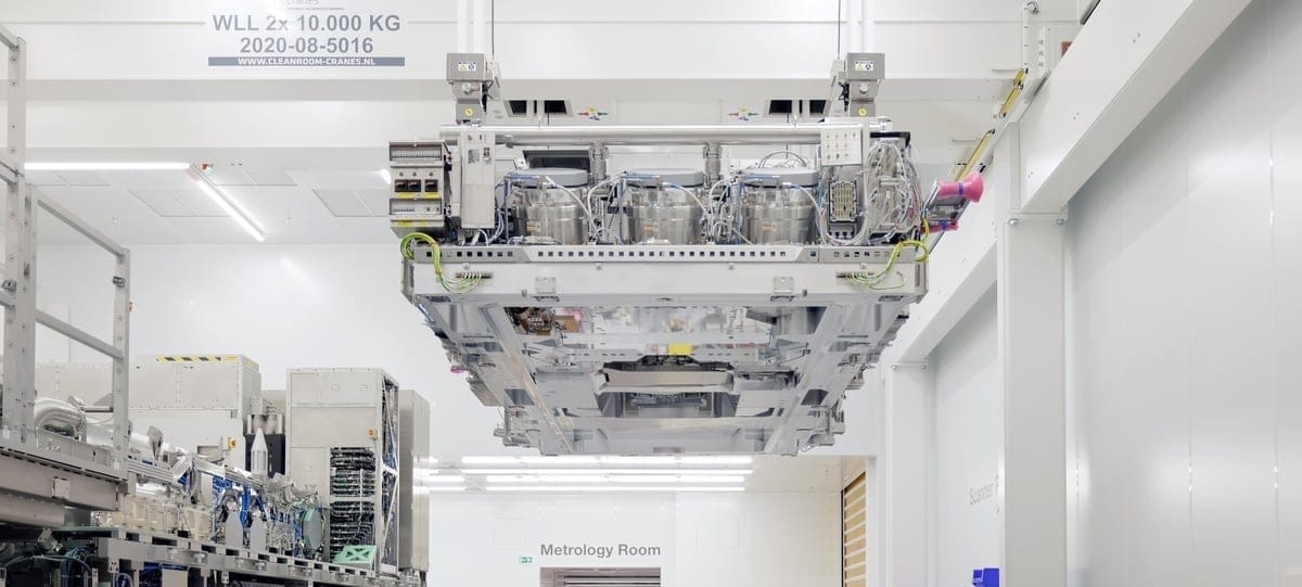
Half-field and stitching. The anamorphic 8x direction halves the field to 26 x 16.5 mm versus the standard 26 x 33 mm full field [12]. Dies larger than the half-field (notably large AI accelerators and GPUs) require field stitching, exposing two half-fields and joining them, which imposes overlay penalties at the stitch boundary and consumes yield. ASML's throughput specification of 175 wafers per hour for the EXE:5200B is quoted without stitching; stitched throughput is lower (the near-term EXE:5200C is described at 190 wph without stitching versus 160 with stitching) [22].
Resolution and k1. High-NA targets 8 nm single-exposure resolution, corresponding to 16 nm lines/spaces pitch, with imec describing an eventual 16-18 nm metal-pitch line/space target and 24-28 nm contact-hole pitch [12][22][24]. At 8 nm half-pitch, k1 = 8 x 0.55 / 13.5 = ~0.33 (modeled from the Rayleigh relationship). imec reported in 2024 that High-NA achieved its theoretical resolution on a wafer, which it characterized as a world record (demonstrated) [33]. imec cautions that the yielding resolution limit for industry-relevant structures will be larger than the 16 nm-pitch optical limit because resist, underlayer, and etch performance, not the aerial image, set the manufacturable floor [24].
Constraints. Depth of focus at 0.55 NA is 2-3x smaller than at 0.33 NA, which is the principal reason resist films must thin below ~30 nm (toward 20 nm and below) to maintain a 2:1 aspect ratio and avoid line collapse [24][13][16]. Source power, dose (the EXE:5200B specification is quoted at 50 mJ/cm2), and stochastics interact: thinner resist absorbs fewer photons, worsening shot-noise-driven stochastic failure exactly where resolution is highest.
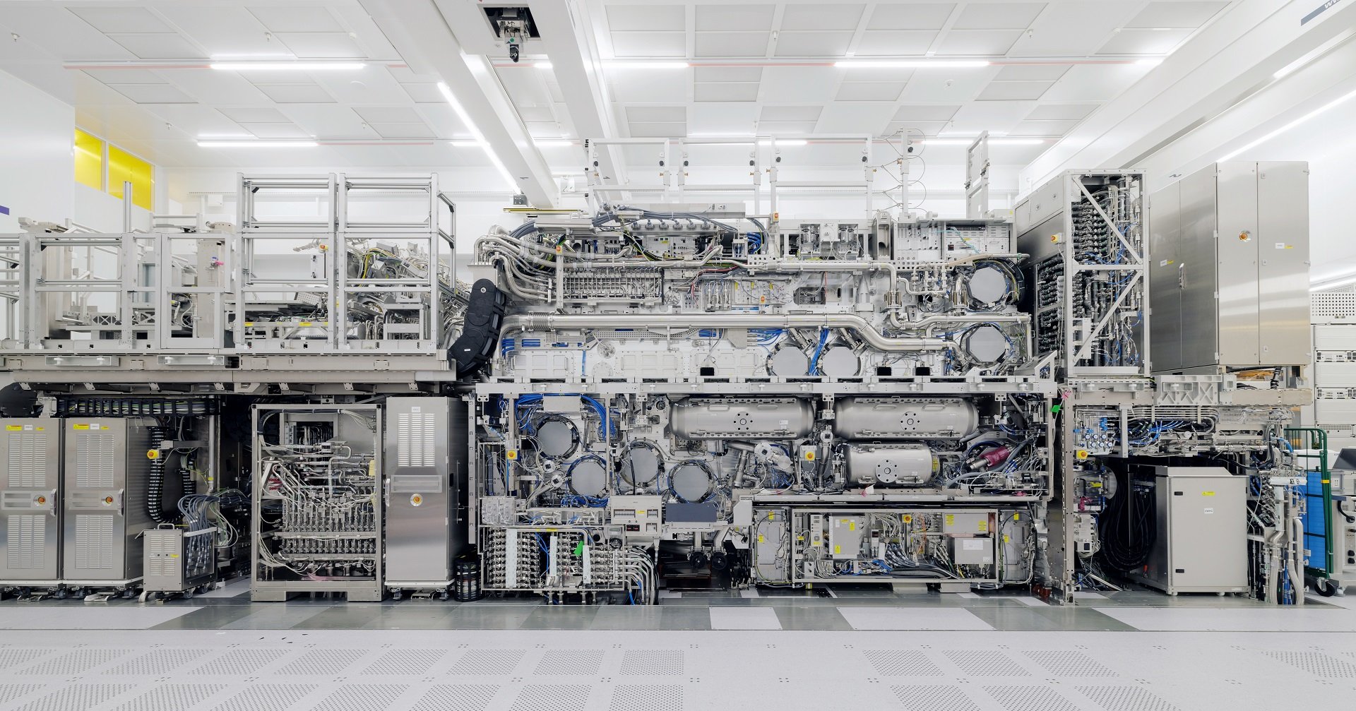
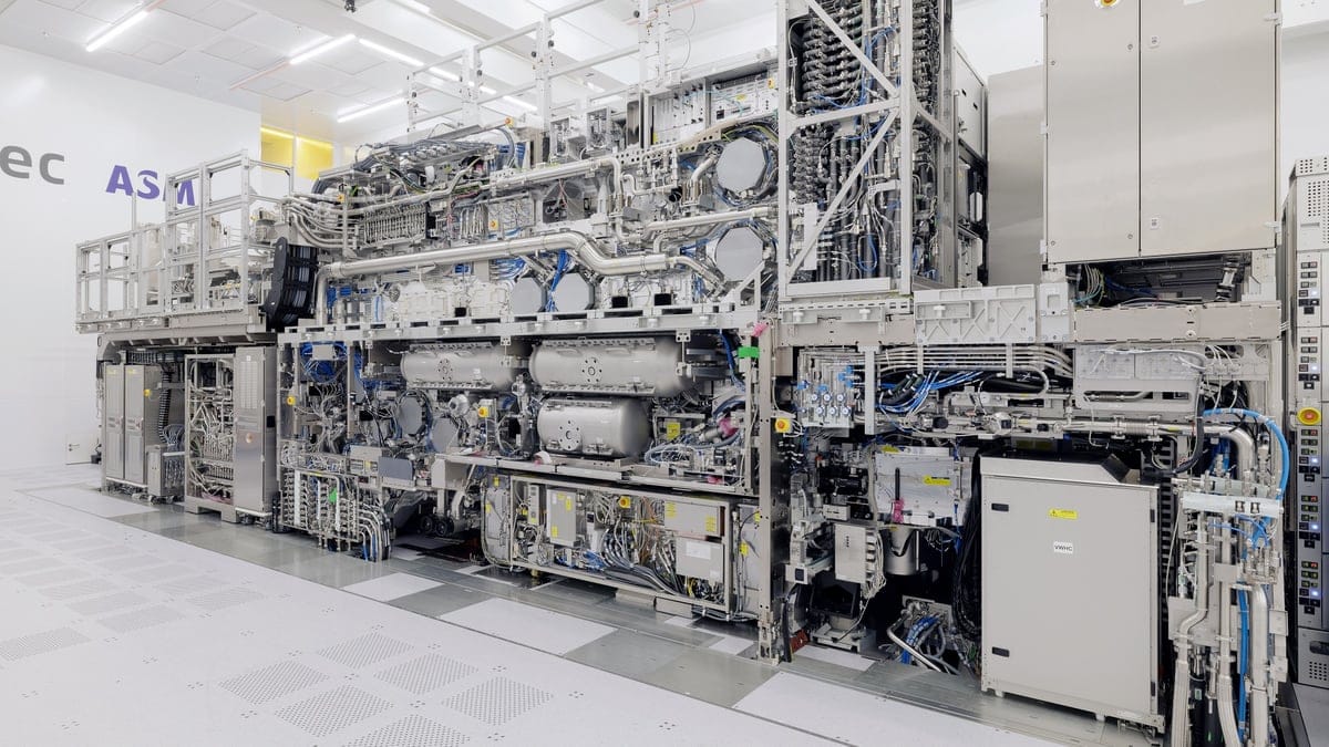
EXE:5000 versus EXE:5200. The EXE:5000 is the early-access/pilot generation, shipping since 2023/2024 for R&D and process development; the EXE:5200B is the high-volume-manufacturing generation, offering a 60% productivity improvement to over 175 wafers per hour and improved overlay of 0.7 nm [5][6][9]. As of the research date the install base comprised five EXE:5000 R&D systems (two at Intel, one each at TSMC and Samsung, and one in the joint ASML-imec High-NA Lab in Veldhoven) followed by EXE:5200B units [6]. SK hynix (KRX: 000660) became the first memory maker to install an EXE:5200B, at its M16 fab in Icheon in September 2025 [9][29]. Samsung Electronics (KRX: 005930) received its first EXE:5200B in October 2025 with a second unit due in the first half of 2026 for its 1.4 nm foundry node. imec took delivery of an ASML EXE:5200 High-NA EUV system expected to be fully qualified by Q4 2026, per imec and TrendForce (March 19, 2026); Reuters put the cost at roughly $400 million and described it as one of fewer than a dozen units worldwide [22]. Intel completed EXE:5200B acceptance testing in December 2025 for its 14A process, with risk production targeted for 2027 [6][9].

3.2 Announced Hyper-NA Generation at ~0.75 NA
ASML placed Hyper-NA on its official roadmap for the first time at imec's ITF World in May 2024, via then-president Martin van den Brink, with a primary target of 0.75 NA (0.85 NA also under study) and a stated availability of around 2030 [19][20][21]. ASML clarified to EE Times that this represents "Martin's vision" and that "feasibility studies are currently ongoing" [19]. Carl Zeiss SMT has begun preliminary lens designs; ASML cannot commit a Hyper-NA product timeline without Zeiss confirming the optics can be designed and manufactured [21]. No Hyper-NA hardware exists; all performance figures are aspirational.
The engineering challenges are credible and severe. imec's Kurt Ronse notes that above 0.55 NA, polarization effects degrade contrast because one polarization orientation effectively cancels the light, requiring polarizers that block photons and reduce efficiency [19][20]. Depth of focus shrinks further; resists must thin beyond High-NA's already-thin films, worsening etch selectivity and stochastics; and an electron-blur floor of roughly 2 nm may impose a resolution barrier independent of optical improvements [20]. Tool cost has been estimated at roughly $720M per system by TrendForce (asserted, not confirmed by ASML) [3][19]. These figures should be treated as roadmap and aspirational, not demonstrated.
4. Axis Two: Pattern-Multiplying and Non-Optical Techniques
4.1 Directed Self-Assembly (DSA)
DSA exploits the microphase separation of block copolymers (BCPs) to form regular features at pitches tighter than the lithographic guide pattern. Two pre-patterning approaches exist: grapho-epitaxy (topographic guide features) and chemo-epitaxy (chemical-contrast guide stripes). The achievable natural pitch is governed by the Flory-Huggins interaction parameter chi: the conventional PS-b-PMMA system has low chi and is limited to roughly 20 nm pitch (about 12-14 nm half-pitch), while high-chi silicon-containing or otherwise polar/fluorinated blocks reach smaller natural pitches [25][26][27].
Demonstrated results. imec demonstrated a low-defectivity, stable PS-b-PMMA process at 28 nm pitch in 2019, and in 2021 at SPIE Advanced Lithography demonstrated 18 nm-pitch line/space patterning with a high-chi BCP under HVM-representative conditions, transferring the pattern into an underlying SiN layer for defectivity inspection [25][30]. High-chi materials were supplied through imec partners including Merck KGaA, Brewer Science, Nissan Chemical, and Tokyo Ohka Kogyo [30].
Barriers. The dominant obstacles to HVM adoption are defectivity (dislocations, bridges, and missing/merged features, which must reach the very low defects-per-square-centimeter levels HVM requires) and line-edge/line-width roughness. High-chi BCPs are also harder to orient perpendicularly than PS-b-PMMA, which anneals readily [27]. DSA's realistic near-term role is complementary rather than substitutive: contact-hole shrink and rectification, and the highly regular arrays of DRAM, are more amenable than the irregular two-dimensional routing of logic. No peer-reviewed source identified during this research established a specific DSA defects-per-square-centimeter figure currently meeting logic HVM requirements; the technology remains a complement to top-down patterning.
4.2 Advanced Multipatterning
Multipatterning decomposes a sub-resolution layer into multiple relaxed-pitch steps. The principal schemes:
- SADP (self-aligned double patterning): a mandrel is patterned, spacers are deposited on its sidewalls, and the mandrel is removed, doubling feature density. Pitch is set by spacer width (highly controllable), relaxing overlay dependence. Used for fin and line/space formation.
- SAQP (self-aligned quadruple patterning): the SADP sequence applied twice, quadrupling density, used in DRAM active/storage-node layers and FinFET fins. Each level adds deposition and etch steps.
- SALELE (self-aligned litho-etch-litho-etch): a hybrid SADP/LELE scheme used for early BEOL metal layers, in production from the 7 nm node (DUV) and continuing at 5 nm (EUV), addressing tight tip-to-tip definition without dummy metal and reducing parasitic capacitance [37][38][39].
Trade-offs. Litho-etch-litho-etch schemes consume overlay budget directly: each additional masked exposure must align to the prior, and overlay error converts directly into edge-placement error (EPE). Self-aligned schemes (SADP/SAQP) relax this because the critical pitch is defined by deposited spacer thickness rather than a second lithographic alignment. Multipatterning's costs are mask count, process-step count, and cycle time; for line patterning at sub-30 nm pitch, however, SADP/SAQP can be preferable to single-exposure EUV precisely because they avoid EUV stochastic missing/bridging failures and use mature, lower-cost tools [39][40]. Lam Research (NASDAQ: LRCX) has modeled SALELE-with-self-aligned-blocks flows for 18 nm and 16 nm metal pitch at the N3 node [37][41]. The central economic question for High-NA adoption is whether single-exposure High-NA undercuts low-NA double patterning on cost per wafer pass; SemiAnalysis estimates that low-NA double patterning may still cost less than High-NA single patterning at matched 8 nm resolution, which underpins TSMC's decision to defer High-NA [22][42].
4.3 Nanoimprint Lithography (Canon)
Canon Inc. (NYSE: CAJ; TSE: 7751) commercialized jet-and-flash imprint lithography (J-FIL) with the FPA-1200NZ2C, released October 13, 2023, the first commercial semiconductor NIL system [44][48]. The tool dispenses resist by inkjet and presses a patterned mask (template) into it, curing under UV; because there is no projection optic, complex 2D/3D patterns transfer in a single imprint, and there is no high-power EUV source [44][48].
Performance and economics. Canon states a 14 nm minimum linewidth (5 nm-node-equivalent), with a roadmap to 10 nm (2 nm-node-equivalent) contingent on mask improvement [48]. Canon CEO Fujio Mitarai has stated NIL power consumption is roughly one-tenth that of EUV and that pricing would be "one digit lower" than EUV (a phrase variously interpreted; Canon executives have separately suggested per-imprint cost could be roughly halved versus projection exposure and that total NIL line equipment investment could be a fraction of an EUV line) [47][49]. Canon shipped an FPA-1200NZ2C to the Texas Institute for Electronics (TIE), supported by the University of Texas at Austin, in September 2024 for advanced R&D and prototyping [44][51].
Limitations and adoption envelope. The decisive obstacles are defectivity and particle sensitivity (every imprint contacts the wafer, risking template damage and defect replication), overlay, throughput, and template (mask) wear/lifetime. The Financial Times has reported analyst views that yield must approach 90% to compete with EUV [49]. NIL masks (1x templates) are themselves difficult to fabricate. The realistic adoption envelope is memory with regular, repetitive structures (3D NAND, selected DRAM) rather than leading-edge logic; named evaluators include Kioxia (formerly Toshiba Memory), which co-developed NIL with Canon and Dai Nippon Printing over roughly a decade, and reportedly SK hynix and Micron (NASDAQ: MU) [44][45][49][52]. Canon's positioning is explicitly a niche, lower-capital alternative rather than an EUV replacement.
5. The Enabling Ecosystem
5.1 Photoresist Platforms and Patterning Stochastics
Three resist families compete along the RLS trade-off triangle (resolution, line-edge roughness, sensitivity), which cannot be simultaneously optimized:
- Chemically amplified resists (CAR): the 193i/EUV workhorse, organic, spin-on, relying on a photoacid-generator cascade. Lower EUV absorption and a random distribution of components contribute to stochastics; struggles to hit sub-14-nm-pitch resolution at manufacturable dose [16][18].
- Metal-oxide resists (MOR): tin-based (Inpria, now a JSR subsidiary), offering high EUV absorption (~20/micron, roughly 4x CAR), short secondary-electron blur, and high etch selectivity (~40:1), enabling ultrathin sub-20-nm films that mitigate pattern collapse; demonstrated to 8 nm half-pitch in early work and 13 nm half-pitch at 35 mJ/cm2 on an NXE:3300B [17][18][35].
- Dry-deposited resist (Lam Research / ASM International (Euronext Amsterdam: ASM)): vapor-phase ALD-deposited organotin films with anisotropic dry development, offering higher uniformity, precise thickness control, and reduced wet-development stochastic defects; 12 nm lines/spaces (24 nm pitch) demonstrated on a 0.33-NA scanner [16][35]. Lam reports engagement with imec, ASML, Samsung, Intel, TSMC, and SK hynix on logic and DRAM commercialization [36].
Stochastic failure modes. EUV stochastics manifest as microbridges, broken/missing lines, and merged/missing contacts, originating in photon shot noise (the discrete, Poisson-distributed arrival of EUV photons), variation in absorbed-photon count, and secondary-electron blur. Because a die contains billions of contacts, failure must be controlled to roughly 7-sigma; measured data show that at 18 nm contacts and 25 mJ/cm2, the 7-sigma absorbed-photon-shot-noise variation is ~17% for a high-absorbance Inpria film versus ~31% for CAR, a direct quantification of MOR's stochastic advantage [34]. High-NA's thinner films and smaller depth of focus reduce absorbed photons per feature, intensifying stochastic sensitivity precisely where resolution gains are sought [13][16].
5.2 Mask and Pellicle Infrastructure
Mask blanks. EUV masks are reflective: a molybdenum-silicon (Mo/Si) multilayer of roughly 40-50 bilayer pairs on an ultra-low-thermal-expansion substrate, each bilayer reflecting ~70% at 13.5 nm, capped with ruthenium [2]. Mask defectivity combines substrate, multilayer (phase), and absorber-pattern defects; buried multilayer phase defects are particularly difficult to detect and may require actinic (at-wavelength) inspection [53][54]. Absorber development is active: conventional tantalum-based absorbers (~60 nm) transmit some light into the multilayer, contributing to mask 3D effects, motivating high-k/low-n and attenuated-phase-shift absorber options (and novel materials such as CrSb for high-NA 3D-effect reduction) [55][57].
Pellicles. EUV pellicles must combine high transmission (>90%, ideally), low reflectance, and survival of rising source power. First-generation polysilicon-based pellicles reached ~83% transmission (ASML) and were not HVM-ready; TSMC has at times run pellicle-free to preserve transmission [58]. Carbon nanotube (CNT) pellicles are the leading high-power solution: imec demonstrated CNT pellicles with single-pass EUV transmission up to 97% on the NXE:3300 scanner (imec press release, October 6, 2020), and the imec-Mitsui Chemicals partnership (December 14, 2023) targets pellicles with EUV transmittance of at least 94% able to withstand EUV power levels beyond 1 kW, aimed at the 2025-2026 high-power timeframe [56][58][59]. At High-NA, the anamorphic mask and half-field change pellicle coverage and thermal-load geometry, and CNT remains the primary candidate.
5.3 Computational and Inverse Lithography
Shrinking k1 forces aggressive reticle enhancement: optical proximity correction (OPC), source-mask optimization (SMO, essential to recover depth of focus at 0.55 NA via sub-resolution assist features), and inverse lithography technology (ILT), which produces curvilinear mask shapes that improve process window and depth of focus [11][60]. Curvilinear ILT explodes the shot count of legacy variable-shaped-beam (VSB) mask writers, making multibeam mask writers (MBMW) essential. IMS Nanofabrication (a private company majority-owned by Intel, which acquired full ownership by 2015; Intel sold ~20% to Bain Capital and ~10% to TSMC in 2023, valuing IMS at ~$4.3B) commercialized the first high-throughput MBMW with a 262,144-programmable-beam architecture, write time under 10 hours independent of pattern complexity [10][61][62][63]. NuFlare (a Toshiba group company) is the second MBMW vendor. ML-accelerated OPC/ILT (e.g., ASML's Brion subsidiary, and tools from Synopsys (NASDAQ: SNPS) and Cadence Design Systems (NASDAQ: CDNS)) reduces the substantial compute cost of full-chip curvilinear correction [22].
5.4 Overlay and Metrology
As features shrink, the edge-placement-error (EPE) budget, the root-sum-square of CD error, overlay, and stochastic line-placement error, becomes the binding constraint. High-NA targets 0.7 nm overlay on the EXE:5200B (asserted/demonstrated in acceptance testing) and sub-0.8/0.7 nm on later variants [6][22]. Self-aligned schemes (SADP/SAQP/SALELE) relax overlay by defining critical pitch with deposited spacers rather than a second aligned exposure, which is a central reason they persist against single-exposure EUV [39][40]. The metrology/inspection toolchain (CD-SEM, optical scatterometry, e-beam inspection, increasingly multibeam e-beam inspection, where ASML reports growing adoption) faces the fundamental difficulty that stochastic defects are rare, randomly located, and require inspecting very large areas at very low defect-density thresholds, straining throughput [1][53].
6. Key Players and Stakeholders
Scanner and optics. ASML Holding N.V. is the sole supplier of EUV and High-NA scanners; Carl Zeiss SMT (private; subsidiary of Carl Zeiss AG) is the sole optics source; Cymer (private; ASML subsidiary) and Trumpf (private) supply the laser-produced-plasma source and drive laser. This is a serial monopoly chain with no redundancy.
Foundries/IDMs. Intel, TSMC, and Samsung Electronics are the three leading-edge logic adopters with divergent High-NA timing (Section 7).
Memory. SK Hynix, Samsung, and Micron Technology, are the DRAM makers; SK Hynix leads in High-NA installation and EUV-layer count.
Materials and equipment. JSR Corporation is now private, taken over by the state-backed Japan Investment Corporation (JIC): JIC's tender via JICC-02 completed in April 2024 and JSR delisted from the Tokyo Stock Exchange on June 25, 2024, in a transaction valued at roughly JPY 900 billion (~$6.3-6.9B); Inpria is a JSR subsidiary [64][65][66][67]. Tokyo Electron (TSE: 8035), Applied Materials (NASDAQ: AMAT), Lam Research (NASDAQ: LRCX), KLA (NASDAQ: KLAC), and Lasertec (TSE: 6920, the dominant EUV mask/blank inspection supplier) round out the toolchain. EDA: Synopsys (NASDAQ: SNPS) and Cadence (NASDAQ: CDNS).
Research institutes. imec (private non-profit, Leuven) is the central pre-competitive R&D hub; the joint ASML-imec High-NA Lab in Veldhoven is the ecosystem proving ground.
China. SMEE / Shanghai Micro Electronics Equipment (state-linked, not publicly listed in the Western sense) is the leading domestic scanner maker; Huawei (private) and Tsinghua University anchor indigenous EUV-source efforts.
7. Economic and Market Dynamics
7.1 ASML System Economics
The EXE:5200B costs roughly $350M-$400M installed, per Reuters and industry reporting (e.g., TrendForce, January 2026); ASML CFO Roger Dassen confirmed in the January 2026 earnings call that ASML shipped its first production-grade EXE:5200B in Q4 2025. This compares with ~$180M for an NXE:3800E 0.33-NA system and an aspirational ~$720M for Hyper-NA [3][8]. ASML told Reuters in early 2024 it had taken 10-20 High-NA orders and planned to deliver 20 systems annually by 2028 [3]. The platform shares its bottom module (wafer handler, stage mechanics) with the NXE line, reducing manufacturing complexity. ASML's standard EUV production rate is roughly 50-60 systems per year, the physical ceiling on global leading-edge capacity addition [21]. In FY2025 ASML recognized revenue on 48 EUV systems (NXE and EXE), with total net sales of EUR 32.7B; full-year 2026 revenue guidance is EUR 36-40B [2][3].
7.2 The Cost-per-Wafer Crossover
The decisive metric is throughput-normalized cost per wafer pass, not resolution. A High-NA tool costs roughly twice a low-NA tool and runs at lower throughput (175 wph versus 195-220+ wph for NXE:3800E), so a single High-NA exposure must displace two-or-more low-NA exposures plus their associated etch/deposition steps to pay off [42]. High-NA wins where it collapses a multi-mask multipatterning stack into one exposure (reducing cycle time, defect-introducing steps, and EPE); it loses where low-NA double patterning achieves the same pitch at lower cost. SemiAnalysis's assessment that low-NA double patterning may remain cheaper than High-NA single patterning at 8 nm resolution is the analytical core of TSMC's deferral [42][22].
7.3 Divergent Adoption Strategies
- Intel: earliest adopter; EXE:5000 since 2023, EXE:5200B acceptance-tested December 2025, deploying High-NA on 14A critical layers with risk production targeted 2027 [6][9]. imec's Ronse attributes Intel's preference to its relatively weaker double-patterning mastery, making higher single-exposure resolution attractive [20].
- TSMC: explicitly deferring; will not use High-NA for A16 or A14, extending 0.33-NA EUV plus multipatterning and computational lithography; SemiAnalysis projects adoption no earlier than the A10 (1 nm-class) node around 2029-2030 [4][7][22][42].
- Samsung: mid-timeline; first EXE:5200B October 2025, second in H1 2026 for its 1.4 nm foundry node and 2 nm lines [22][29].
- DRAM (SK hynix, Samsung, Micron): SK hynix leads, installing the first memory High-NA tool (M16, September 2025) and moving to five-or-more EUV layers in 1c (sixth-generation 10 nm-class) DRAM; Micron uses EUV in its equivalent 1-gamma DRAM; all three are investing heavily in 1c DRAM for AI/HBM demand [9][28][31][32]. High-NA's DRAM ROI is contested: one industry view holds the move is partly a "we are first" positioning given that planar DRAM scaling is stalling against 6F2/4F2 geometric limits and 3D DRAM is the more consequential roadmap inflection [29][32].
8. Regulatory Landscape
Export controls are a material, not peripheral, dimension. EUV systems have been barred from China since 2019 via US-Dutch coordination [69][70]. The control perimeter has since widened to advanced DUV: the Netherlands required licenses for the most advanced immersion systems (TWINSCAN NXT:2000i and above) from 2023-2024, and in September 2024 brought ASML's 1970i/1980i immersion DUV tools under Dutch licensing, shifting ASML's filing obligation from the US to The Hague [69][71][72]. A further Dutch tightening on measurement/inspection equipment took effect April 1, 2025, closely aligned with US measures [73]. The Dutch regime is country-neutral and case-by-case rather than a blanket ban; as many as 41 Chinese entities reportedly held valid DUV import licenses, and ASML continued servicing installed Chinese equipment under license [69].
US Bureau of Industry and Security (BIS) controls (the October 2022 package and subsequent updates) target advanced logic/memory equipment and "booster" technologies (notably US etch/deposition tools) that allow older DUV plus multipatterning to reach 7 nm-class nodes [70]. Japanese measures, effective July 2023, require licenses for 23 categories of chipmaking equipment, and Japan's photoresist supply (JSR, Tokyo Ohka Kogyo, Shin-Etsu, Sumitomo, Fujifilm, collectively ~90% of global photoresist) is a parallel bottleneck, reinforced by JIC's take-private of JSR [70][68]. A US bill, the proposed MATCH Act, would prohibit ASML sales to China entirely; China's share of ASML's global sales fell to 33% in 2025 from 41% in 2024 (ASML FY2025 report, via SCMP, January 28, 2026), with CFO Roger Dassen expecting it to drop to ~20% in 2026, so full enforcement would materially affect ASML revenue [76]. This sub-area on the precise reach of the newest 2025-2026 BIS rules is thinner in public sourcing than the 2023-2024 actions, and is flagged as such.

9. Geopolitical and Strategic Dimensions
9.1 Industrial Policy
The US CHIPS and Science Act mobilized roughly $52B in direct funding; as of January 2025 it had awarded ~$33.7B in grants and ~$5.5B in loans [74][75]. Among upstream-supply awards, the US Department of Commerce/NIST finalized up to $458 million in direct funding to SK hynix on December 19, 2024, supporting SK hynix's approximately $3.9 billion investment in an HBM advanced-packaging and R&D facility in West Lafayette, Indiana, plus up to $500M in loans [75]. The EU Chips Act aims to mobilize ~EUR 43B toward a 20% global-share-by-2030 target; the European Commission directly controls only EUR 4.5 billion (about 5%) of the roughly EUR 86B in estimated Chips Act funding through 2030, with the remainder coming from member states and industry (ECA Special Report 12/2025) [77]. The European Court of Auditors found in Special Report 12/2025 (published April 28, 2025) that the Chips Act is "very unlikely to be sufficient" to reach the 20% target, citing the Commission's own July 2024 forecast that the EU share rises only from 9.8% in 2022 to just 11.7% by 2030; audit member Annemie Turtelboom characterized the 20% target as "essentially aspirational" [77]. Intel's July 2025 cancellation of its ~EUR 30B Magdeburg fab was a significant setback, and a Chips Act 2.0 was proposed June 2026 [77][78]. Japan (~EUR 16.7B grants), South Korea's K-Semiconductor Belt, and Taiwan (~EUR 16.7B tax incentives) round out the subsidy race, against China's reported ~EUR 135B equity deployment [78].
9.2 Single-Point-of-Failure Concentration
The supply chain exhibits extreme concentration: one scanner supplier (ASML), one optics source (Carl Zeiss SMT), concentrated LPP-source supply (Cymer/Trumpf), concentrated resist supply in Japan, concentrated mask-blank and pellicle supply (largely Japan: Hoya, AGC, Mitsui), and concentrated mask-inspection (Lasertec). Any single failure, geopolitical, natural-disaster, or technical, propagates across the entire leading edge with no substitute.
9.3 China's Indigenous Lithography Efforts
SMEE remains the leading Chinese scanner maker but is generations behind at the leading edge (publicly credited with ~90 nm-class production tools, with DUV ambitions). Reported indigenous EUV efforts pursue two tracks. The first is a laser-induced discharge plasma (LDP) source (associated with Harbin Institute of Technology, Huawei, and SMEE), reportedly reaching 100-150 W in mid-2025 per low-reliability trade reporting (sufficient for "first light," below the 250 W+ for HVM); these claims circulate primarily via low-quality aggregators and should be treated as unverified [85][86]. Reports of a "validated domestic EUV prototype" in late 2025 are not credible as stated [85].
The second track, steady-state microbunching (SSMB) EUV, has a genuine, peer-reviewed foundation and warrants careful labeling. The SSMB concept originated with Ratner and Chao (Phys. Rev. Lett. 2010) [87]. A 2021 proof-of-principle, a Tsinghua University-HZB-PTB collaboration conducted at the Metrology Light Source storage ring in Berlin and published in Nature (Deng, Chao, Tang et al.), demonstrated (measured) laser-induced microbunching and coherent radiation one revolution after modulation, at infrared/visible wavelengths (1064 nm fundamental, 532 nm harmonic), with unconfined microbunches; this was not true steady state and produced no EUV [88]. A 2024 follow-up in Communications Physics (Kruschinski, Deng, Chao et al.) confirmed the underlying theory and the controllability of transverse-longitudinal coupling, while explicitly noting large shot-to-shot intensity fluctuations and that true steady state requires building a prototype accelerator facility, described as in active design study at Tsinghua [89]. A kilowatt-class EUV design (>1 kW at 13.5 nm, <2% bandwidth, ~100-160 m ring) is modeled/simulated (Scientific Reports 2022 and Tsinghua design studies), not demonstrated [90]. Reported site selection occurred in Xiong'an in February 2022; claims that facility construction began in early 2025 are unsourced and not credible [91]. Independent assessments (eeNews Europe 2023; other analyses) judge SSMB-EUV to be 15-20 years from practical lithography use, if ever, because the source is only one of several unsolved problems (optics, masks, resists remain), placing it well outside the commercial roadmap window [92]. SSMB-EUV is, on current evidence, research-stage and speculative as a manufacturing technology.
10. Risk Matrix
| Risk | Likelihood | Impact | Mitigations |
|---|---|---|---|
| High-NA throughput / stochastic-yield shortfall (175 WPH and 0.7 nm overlay not sustained in HVM; thin-resist stochastics cap practical resolution) | Moderate | High — undermines the High-NA economic case and may delay advanced-node production ramps. | High-absorbance metal-oxide and dry resists; SMO and ILT for depth-of-focus recovery; stitching-free die design; staged deployment on only the most critical layers. |
| Single-supplier concentration (ASML lithography and Zeiss optics) | High (structural) | Severe — disruption could halt progress at the global leading edge. | Strategic tool inventories; extended low-NA utilization as a hedge; geographic diversification of installed systems; long-term service and support agreements. |
| Export-control disruption (MATCH Act, BIS/Dutch/Japanese restrictions, Chinese material retaliation) | Moderate | Moderate–High — revenue pressure and supply-chain friction, particularly for China-exposed suppliers. | Revenue diversification; compliance infrastructure; allied supply redundancy; contingency planning for a complete China cutoff. |
| Nanoimprint defectivity and overlay limitations (yield unable to approach ~90% competitiveness; template wear issues) | Moderate | Low–Moderate — primarily affects memory applications rather than the most advanced logic nodes. | Restrict deployment to regular memory layers; invest in template inspection and repair; maintain strict particle control; treat NIL as a cost-reduction hedge rather than a primary scaling path. |
| Resist-stochastics fundamental limit (electron blur around ~2 nm imposes a practical resolution floor) | Moderate | High — limits Hyper-NA benefits and raises dose and manufacturing cost. | Single-component small-molecule resists; dry-resist systems; dose-versus-throughput optimization; stochastic-aware OPC and computational lithography. |
| Cost-per-wafer crossover fails to materialize (low-NA multipatterning remains economically superior) | Moderate | High — negative for High-NA adoption, favorable for multipatterning tool vendors. | Layer-specific deployment strategies; throughput roadmap execution (EXE:5200C/D, 5400E, 5600); design-rule co-optimization to maximize single-exposure routing benefits. |
| Hyper-NA feasibility failure (polarization, depth-of-focus, and optics challenges remain unsolved at acceptable cost by ~2030) | Moderate | Moderate — roadmap delays rather than an immediate production risk. | Continue extending low-NA and High-NA EUV; maintain Beyond-EUV and e-beam lithography research programs; require Zeiss feasibility milestones before major capital commitments. |
11. Strategic Recommendations
11.1 For Foundry and IDM Technology Strategists
- Treat High-NA as a layer-level cost decision, not a node-level commitment. Adopt High-NA only on layers where one exposure replaces two-or-more low-NA exposures plus their etch/deposition overhead and where stitching is avoidable. The benchmark that should change the decision: when High-NA throughput-normalized cost per wafer pass at production yield falls below low-NA double-patterning cost at matched pitch. Until then, extend 0.33-NA EUV with SALELE/SADP and computational lithography, as TSMC is doing.
- Invest now in the resist and stochastics stack. Because yielding resolution, not optical resolution, is the binding limit, qualify high-absorbance MOR and dry resist in parallel with tool installation. Track 7-sigma defect-rate behavior at target dose as the readiness gate.
- Design for the half-field. Re-architect large dies (AI accelerators) for sub-26x16.5 mm reticle fields or robust stitching before High-NA volume, since stitching overlay penalties directly erode the High-NA yield case.
11.2 For Capital Planners
- Model the full cost of ownership, not the sticker price. A roughly $350-400M installed tool at 175 wph with 2-3x worse depth of focus and thinner-resist yield risk must be evaluated on cost per good wafer pass over a multi-year ramp, including pellicle, mask, and metrology infrastructure. Avoid resolution-driven capital commitments.
- Stage commitments against ASML's throughput roadmap. Defer large High-NA fleet purchases until the EXE:5200C/D and 5400E throughput/overlay improvements (190-210 wph, sub-0.7-0.8 nm overlay) are demonstrated, unless first-mover process-leadership value (Intel's case) justifies the premium.
11.3 For Institutional Investors and Corporate Strategists
- Price the ASML/Zeiss monopoly as both moat and concentration risk. The serial monopoly chain is a strong position in semiconductors and simultaneously the supply chain's gravest single point of failure; weight both. Monitor China revenue exposure (33% in 2025, guided toward ~20% in 2026) against MATCH Act and BIS/Dutch developments as the key downside catalyst.
- Recognize the materials bottleneck moved off public markets. With JSR private under JIC and Inpria inside it, the highest-leverage resist exposure is no longer directly investable; favor adjacent public proxies (Tokyo Electron, Lam Research, Lasertec, ASM International) for resist-process and inspection exposure.
- Discount disruptive-source narratives. Treat Chinese SSMB-EUV and Beyond-EUV as 15-20-year research options, not near-term competitive threats; nanoimprint as a memory-niche optionality (Canon), not an EUV displacer. None changes the leading-edge competitive structure within the commercial roadmap horizon.
12. Horizon Scan Beyond Hyper-NA
Beyond-EUV (6.x nm). A shorter wavelength near 6.5-6.7 nm (gadolinium emits near 6.7 nm, terbium near 6.5 nm, via 4f-4d unresolved-transition-array emission) would extend optical resolution further [80][81][82]. The barriers are fundamental and unsolved: no industry-standard high-power 6.x nm source exists; candidate La/B4C or Mo/B4C multilayer mirrors currently reach ~40% reflectivity (theoretical max >70%) with a narrow ~0.6% bandwidth versus 2% for Mo/Si at 13.5 nm; and there is no resist, mask, or component ecosystem [81][82][83][84]. Fraunhofer ILT/IOF have run a "Beyond EUV" program generating 6.7 nm output [81]. This is research-stage and not a commercial-roadmap-window technology.
Multibeam e-beam. Multibeam mask writing is mature and in production (IMS, NuFlare). Maskless e-beam direct write, however, remains throughput-limited: industrial 300 mm direct write at ~100 wph requires beam currents >2 mA, far beyond demonstrated multibeam capability; practical systems achieve single-digit-to-~25 wph per module and are confined to mask writing, prototyping, small-volume, and advanced-packaging niches [62][79]. It is a complementary, not displacing, technology within the horizon.
Alternative high-power sources. SSMB and free-electron-laser/energy-recovery-linac concepts (KEK in Japan estimates ~$260M for a 10 kW multi-tool EUV-FEL system) are credible long-term source research but face the same non-source ecosystem barriers; none is a commercial-window manufacturing input [92].

References
[1] ASML Holding N.V. 2025. Form 6-K, Q2 2025 Investor Presentation. Veldhoven: ASML.
[2] ASML Holding N.V. 2026. Form 6-K, FY2025 Results Presentation (January 28, 2026). Veldhoven: ASML.
[3] Shilov, Anton. 2026. "ASML's Roadmap for Chipmaking Lithography Tools Examined." Tom's Hardware.
[4] TrendForce. 2025. "ASML Confirms First High-NA EUV EXE:5200 Shipment." TrendForce News, July 17.
[5] All About Industries. 2025. "With ASML's New EXE Generation, High-NA EUVL Is Ready for Practical Use."
[6] SemiWiki. 2025. "Intel Completes Installation of EXE:5200B High-NA EUV Tool."
[7] TechPowerUp. 2026. "TSMC Says Low-NA EUV Will Carry It Further, Delaying High-NA Adoption."
[8] SemiAnalysis. 2025. "High-NA Is Here (for R&D), EUV Cost, Hyper-NA." SemiAnalysis Newsletter (SPIE 2025).
[9] Bits&Chips. 2025. "Intel Completes Acceptance Testing of ASML's EXE:5200B High-NA EUV Scanner."
[10] Intel Corporation. 2023. "Intel to Sell Minority Stake in IMS Nanofabrication Business to TSMC." Intel Newsroom, September 12.
[11] LaPedus, Mark. 2017. "Multi-Beam Market Heats Up." Semiconductor Engineering.
[12] Heil, Tilmann, et al. 2015. "Anamorphic High NA Optics Enabling EUV Lithography with Sub-8nm Resolution." EUVL Symposium, Maastricht.
[13] imec. n.d. "High-NA EUV Lithography: The Next Step after EUVL." imec.
[14] van Schoot, Jan, et al. 2016. "EUV High-NA Scanner and Mask Optimization for Sub-8nm Resolution." Proc. SPIE.
[15] Semiconductor Engineering. n.d. "Multi-Patterning EUV vs. High-NA EUV."
[16] Derbyshire, Katherine. n.d. "Many Options for EUV Photoresists, No Clear Winner." Semiconductor Engineering.
[17] Meyers, Stephen T., and Andrew Grenville. 2016. "Metal Oxide EUV Photoresists for N7." EUVL Workshop, P79.
[18] Stowers, Jason. 2017. "Metal Oxide Photoresists." EUVL Workshop, P50.
[19] Clark, Don. 2024. "ASML Aims for Hyper-NA EUV, Shrinking Chip Limits." EE Times.
[20] SemiWiki. 2024. "ASML Aims for Hyper-NA EUV, Shrinking Chip Limits" (discussion with imec's Kurt Ronse).
[21] SemiconductorX. 2026. "ASML Spotlight: EUV Monopoly, High-NA, Zeiss Optics & Export Controls." [22] Shilov, Anton. 2026. "ASML's Roadmap for Chipmaking Lithography Tools Examined" (EXE roadmap variants). Tom's Hardware.
[23] PatSnap. 2026. "ASML EUV and High-NA Lithography Technology Roadmap."
[24] imec. n.d. "The Case for High NA EUV: Unlocking the Next Era of Chip Manufacturing." [25] imec. 2021. "Imec Demonstrates 18nm Pitch Line/Space Patterning with a High-Chi Directed Self-Assembly Process." Press release, February 25. [26] U.S. Patent 10,421,878. "High-Chi Block Copolymers for Directed Self-Assembly."
[27] U.S. Patent 11,078,337. "High-chi Block Copolymers for Directed Self-Assembly."
[28] Castellano, Robert. 2025. "SK Hynix First to Install High-NA EUV in DRAM." Substack.
[29] SemiWiki. 2025. "SK Hynix Adopts Next-Generation HNA-EUV ASML Production Equipment for DRAM."
[30] Cao, Y., et al. 2020. "Directed Self-Assembly of Block Copolymers for Sub-10 nm Fabrication." Int. J. Extreme Manuf. 2: 032006. [31] Digitimes. 2025. "SK Hynix Expands EUV in 1c DRAM."
[32] SemiWiki. 2025. "The Three Major Memory Powerhouses Are Investing in 1c DRAM."
[33] imec. 2026. "How High NA EUV Lithography Reshapes the Future."
[34] Fallica, R., et al. 2016. "Absorption of EUV Resists." Proc. SPIE 9776-39 (as cited in Meyers and Grenville 2016).
[35] Semiconductor Engineering. 2025. "Key Technologies to Extend EUV to 14 Angstroms."
[36] SemiAnalysis. 2021. "Lam Research, Tokyo Electron, JSR Battle It Out in the EUV Photoresist Market."
[37] Chen, Frederick. 2020. "SALELE Double Patterning for 7nm and 5nm Nodes." LinkedIn.
[38] U.S. Patent 11,239,077. "Litho-Etch-Litho-Etch with Self-Aligned Blocks."
[39] Wikipedia. n.d. "Multiple Patterning."
[40] Sturtevant, John, et al. 2021. "Defect Characterization of EUV SALELE Patterning Scheme for Advanced Nodes." Proc. SPIE 11611, 116112H.
[41] Lam Research. n.d. "Overcoming BEOL Patterning Challenges at the 3-nm Node: Process Simulation and EPE Control."
[42] SemiAnalysis. 2025. "High-NA vs. Low-NA Multipatterning" (cost analysis). SemiAnalysis.
[44] Canon Inc. 2024. "Canon Delivers FPA-1200NZ2C Nanoimprint Lithography System to the Texas Institute for Electronics." Canon Global News, September 26.
[45] SemiWiki. 2023. "Canon to Compete with ASML? A Two-Horse Race?"
[47] Diskmfr. 2024. "Breakthrough: Canon Nanoimprint Lithography Equipment."
[48] Canon Inc. n.d. "FPA-1200NZ2C." Canon Global product page.
[49] Digitimes. 2024. "Canon Expects to Ship Nanoimprint Lithography Machines by 2024."
[51] Canon U.S.A. 2024. "Canon Inc. Delivers FPA-1200NZ2C NIL System to the Texas Institute for Electronics."
[52] TrendForce. 2024. "Canon Delivers Nanoimprint Lithography System to TIE." [53] Pang, Linyong, et al. n.d. "EUV Mask Defects and Their Removal." ResearchGate.
[54] "Assessing EUV Mask Defectivity." n.d. ResearchGate.
[55] Chen, Frederick. n.d. "The Uncertain Phase Shifts of EUV Masks." LinkedIn.
[56] imec. 2023. "Imec and Mitsui Partner to Commercialize CNT Pellicle." Press release, December 14.
[57] PatSnap. 2026. "EUV Lithography Mask Technology 2026."
[58] LaPedus, Mark. n.d. "EUV Pellicles Finally Ready." Semiconductor Engineering.
[59] imec. 2020. "Imec Demonstrates CNT Pellicle Utilization on EUV Scanner." Press release, October 6.
[60] Tomandl, Mathias, et al. 2024. "Multi-Beam Mask Writing Opens Up New Fields of Application." J. Micro/Nanopattern. Mater. Metrol. 23(1): 011205.
[61] Klein, Christof, Hans Loeschner, and Elmar Platzgummer. 2016. "MBMW-101: World's 1st High-Throughput Multi-Beam Mask Writer." Proc. SPIE BACUS.
[62] Platzgummer, Elmar, Christof Klein, and Hans Loeschner. 2013. "Electron Multibeam Technology for Mask and Wafer Writing at 0.1 nm Address Grid." J. Micro/Nanolith. MEMS MOEMS 12(3): 031108.
[63] Semiconductor Engineering. n.d. "Deploying Multi-Beam Mask Writers."
[64] Private Markets News. 2024. "The Japanese Lock on Photolithography."
[65] Digitimes. 2024. "Japan's JIC Successfully Acquires JSR with Delisting Expected by Summer."
[66] SemiWiki. 2024. "Government-Backed Japan Investment Corporation (JIC) Completes Takeover of JSR." [67] PortersFiveForce. 2024. "Who Owns JSR Company?"
[68] Nomura Securities, cited in Digitimes 2024 (JSR ~27% global photoresist share). [69] AI Policy Bulletin. 2025. "Dutch Export Controls Don't Go Far Enough on China."
[70] Domino Theory. 2024. "Dutch Aim to Create Strategic Autonomy with Chip Gear Export Controls."
[71] ASML Holding N.V. 2024. "Statement Regarding Dutch Government's Updated Export License Requirement." September. [72] TechNode. 2023. "ASML's Export to China Valid Until Year-End."
[73] SemiWiki. 2025. "Netherlands Tightens Export Controls on Sanctioned Semiconductor Equipment."
[74] CSIS. 2024. "A World of Chips Acts: The Future of U.S.-EU Semiconductor Collaboration."
[75] U.S. Department of Commerce / NIST. 2024. "Biden-Harris Administration Finalizes CHIPS Incentives Award with SK hynix." December 19. (Up to $458M direct funding; ~$3.87B SK hynix investment, West Lafayette, Indiana; up to $500M loans.) [76] Bruegel. 2026. "Revamping Europe's Chips Strategy: Indispensability, Not Self-Sufficiency"; ASML FY2025 report via South China Morning Post, January 28, 2026. [77] European Court of Auditors. 2025. Special Report 12/2025: The EU's Strategy for Microchips. April 28; European Commission, "European Chips Act" and "Chips Act 2.0."
[78] Wikipedia. n.d. "European Chips Act."
[79] LaPedus, Mark. n.d. "Multibeam Obtains Funding for Next-Gen E-Beam Lithography." Substack.
[80] Otsuka, T., et al. 2012. "A 6.7-nm Beyond EUV Source as a Future Lithography Source." Proc. SPIE 8322.
[81] Optics.org. n.d. "Fraunhofers Unite to Reduce EUV Wavelengths."
[82] Higashiguchi, Takeshi, et al. n.d. "Shorter-Wavelength Extreme-UV Sources Below 10nm." SPIE Newsroom.
[83] SCIRP. n.d. "Extendibility Evaluation of Industrial EUV Source Technologies for kW Average Power and 6.x nm Wavelength Operation."
[84] Kuznetsov, D. S., et al. 2015. "High-Reflectance La/B-Based Multilayer Mirror for 6.x nm Wavelength." Opt. Lett. 40: 3778-3781.
[85] FinancialContent (TokenRing AI). 2025. "China's Secret Lithography Race." [Low-reliability aggregator; cited only to characterize unverified claims.]
[86] Springer. 2025. "Steady-State Microbunching Based on Transverse-Longitudinal Coupling." Nucl. Sci. Tech.
[87] Ratner, D., and A. Chao. 2010. "Steady-State Microbunching in a Storage Ring for Generating Coherent Radiation." Phys. Rev. Lett. 105: 154801.
[88] Deng, Xiujie, Alexander Chao, Jörg Feikes, et al. 2021. "Experimental Demonstration of the Mechanism of Steady-State Microbunching." Nature 590 (7847): 576-579. DOI 10.1038/s41586-021-03203-0.
[89] Kruschinski, Arnold, Xiujie Deng, Jörg Feikes, et al. 2024. "Confirming the Theoretical Foundation of Steady-State Microbunching." Communications Physics 7: 160. DOI 10.1038/s42005-024-01657-y.
[90] "A Synchrotron-Based Kilowatt-Level Radiation Source for EUV Lithography." 2022. Scientific Reports 12: 7323. DOI 10.1038/s41598-022-07323-z.
[91] South China Morning Post. 2023. "China Plans to Build a Giant Chip Factory Driven by Particle Accelerator."
[92] Clarke, Peter. 2023. "China's Synchrotron EUV Lithography Light Source Is No Sanctions Buster." eeNews Europe, September 25.