Can China Make 5nm Chips Without EUV? SMIC's SAQP Path, Huawei's LogicFolding, and What Stays Blocked to 2031
SMIC reaches 5nm-class density with SAQP multipatterning at 30-50% yield and 2-3x cost. What that serves, and what stays blocked through 2031.

China's Post-EUV Semiconductor Stack, 2026-2031: A Feasibility Assessment of SAQP Multipatterning, Directed Self-Assembly, Nanoimprint Lithography, Huawei's LogicFolding Architecture, CFET and Backside Power Delivery, and Domestic Immersion DUV/EUV Tooling
TL;DR
- China can plausibly manufacture logic at genuine 5nm-class physical density (contacted gate pitch near 51 nanometers, roughly 130-140 MTr/mm²) through 2031 only via SAQP multipatterning on its installed ASML immersion base at 30-50 percent yield and 2-3x merchant cost per good die, output that is viable for state-procured AI accelerators and CPUs but not for export mobile SoCs; true 2nm-class single-die logic at commercial cost and volume is structurally blocked [1][47].
- The alternative patterning routes are misclassified in popular coverage: directed self-assembly and nanoimprint are memory-array-and-photonics tools structurally unsuited to high-volume random logic, and domestic EUV is limited not by its light source but by mask blanks, pellicles, resists, and metrology, a supply-chain-wide co-development problem placing an integrated tool no earlier than roughly 2030 [14][19][40].
- The accessible offsets, backside power delivery (worth about half a node), chiplet-plus-hybrid-bonding packaging, and domestic HBM, are where sustained state investment returns the most defensible capability; Huawei's LogicFolding is a system-and-packaging density-recovery program with an unproven, thermally constrained 3D-logic endpoint, not a demonstrated architecture that substitutes for a node [8][20][43].
Key Findings
The single most important calibration is that SMIC's most advanced shipping process, N+3, is a heavily multipatterned 7nm-class process reaching TSMC N6-class density, not a 5nm-class process. The June 14, 2026 SemiAnalysis STEEL teardown of Huawei's HiSilicon Kirin 9030 measured a 32.5 nanometer minimum metal pitch, a 57 nanometer contacted gate pitch identical to TSMC N6's, a 228 nanometer (5.7-track) cell height, a 30-32 nanometer fin pitch, and a transistor density of 113.4 MTr/mm² against N6's 107.7 MTr/mm², explicitly trailing Intel's 18A high-density library by 38 percent [1]. The "5nm" designation applied by SMIC and Chinese state media therefore diverges from the physical parameters that "5nm-class" denotes at TSMC or Samsung by roughly one full node; the label is a marketing generation, not a measured density [1].
From this calibration, the report reaches an explicit five-dimensional verdict on each path. SAQP is shipping, tool-and-materials-available on the installed immersion fleet, yield-limited to roughly 30-50 percent, cost-penalized at 2-3x merchant, and already at volume. DSA is physically feasible only for regular arrays, structurally blocked for logic by defectivity. NIL is resolution-capable but defectivity- and overlay-limited, suited to memory/photonics/power, and likely export-foreclosed. Domestic immersion is a 28nm-class supply hedge, not a near-term capability expansion, with sub-10nm not before roughly 2030. Domestic EUV is source-advancing but integrated-tool-blocked before roughly 2030 by the mask/pellicle/metrology layer. Monolithic CFET is structurally blocked within the window; backside power delivery is the most accessible offset; advanced packaging and domestic HBM are the most defensible substitutions, with a ceiling at per-transistor energy efficiency.
Details
1. Anchoring the Node Labels
Node names are marketing generations, so capability must be anchored to disclosed parameters. A 5nm-class process denotes a contacted gate pitch of approximately 48-51 nanometers, a minimum metal pitch near 28-30 nanometers, a high-density SRAM bit cell of about 0.021 square micrometers, and a 2-fin logic density near 130-140 MTr/mm²; TSMC N5 measures a 51 nanometer CGP, a 28 nanometer minimum metal pitch, a 0.021 square micrometer HD SRAM cell, and roughly 137 MTr/mm² in dense libraries, with whole-chip mixed density on shipping Apple silicon near 130-135 MTr/mm² [33][34]. A 3nm-class process (TSMC N3E) lifts logic density substantially while delivering little SRAM scaling, its HD SRAM cell remaining near 0.021 square micrometers, an important structural fact for cache-heavy AI designs [34]. A 2nm-class process (TSMC N2) introduces gate-all-around nanosheets, finally shrinks the HD SRAM cell toward 38 megabit per square millimeter, and is where backside power delivery (TSMC A16 Super Power Rail) enters [34].
Against these anchors, SMIC N+3's 32.5 nanometer minimum metal pitch is a single 128 nanometer mandrel divided by four through SAQP, and its density comes from design-technology co-optimization, fin depopulation to two fins per transistor, contact-over-active-gate, and single diffusion break, not from a lithographic generation [1]. Everything downstream about yield, cost, and application follows from the fact that China's leading shipping logic is a multipatterned N6-equivalent.
2. Actors, Installed Base, and Financing
SMIC (HKG:0981), majority state-influenced through China's national IC investment funds, is the only Chinese entity shipping sub-14nm logic in volume. Huawei, a privately held but heavily state-supported national champion, is both the dominant fabless customer through its HiSilicon arm and, through affiliates, a coordinator of the domestic tool effort. The lithography ecosystem comprises SMEE (state-owned, established 2002), the startup Yuliangsheng (added to the US Entity List in late 2024, reportedly Huawei-linked), a state-assembled vehicle reported as Aishengna or AMIES that absorbed SMEE and Yuliangsheng engineering teams, and SiCarrier (state-backed, reportedly Huawei-controlled, holding multipatterning patents) [5][23][24]. Naura (SHE:002371) and AMEC (SSE:688012) supply comparatively strong etch, deposition, and CMP; metrology and inspection remain thin. The memory principals are CXMT (ChangXin Memory Technologies) in DRAM and HBM, pursuing a Shanghai STAR Market IPO seeking 29.5 billion yuan (approximately 4.4 billion dollars, the second-largest STAR listing ever, cleared listing-committee review on May 27, 2026), and YMTC (Yangtze Memory) with its foundry affiliate XMC in 3D NAND and HBM packaging [30][31][32].
These firms are funded to exist at the leading edge rather than to be profitable. SMIC's 7nm-and-below combined capacity was reported at roughly 45,000 wafers per month at the end of 2025, targeted at 60,000 in 2026 and 80,000 in 2027, corroborated across Chinese-industry and UBS estimates [27]. That capacity runs overwhelmingly on ASML (NASDAQ:ASML) immersion scanners acquired before and through the tightening of controls; ASML ships on the order of 130 immersion systems per year industry-wide and holds an estimated 98.7 percent immersion share, so the Chinese advanced immersion fleet is a modest, finite, servicing-constrained asset [23][24]. Goldman Sachs modeling, reported by the South China Morning Post, assumes SMIC adds monthly capacity of 30,000-50,000 advanced-node wafers each year from 2026 to 2031, with yields rising from 23 percent in 2026 to 50 percent in 2030 and 75 percent by 2035, an explicitly modeled projection, not a disclosure [26].


3. Patterning Path Assessment
SAQP and higher-order multipatterning: shipping, yield-limited. From first principles, a 193 nanometer immersion scanner at 1.35 numerical aperture resolves a single-exposure half-pitch of k1·λ/NA; at a manufacturable k1 near 0.28-0.30 this yields a minimum printable pitch of about 76-80 nanometers, roughly a 38 nanometer half-pitch, consistent with the rule that 193i prints about 36-38 nanometer lines without multipatterning [24]. Self-aligned double patterning halves this; SAQP quarters the mandrel pitch, reaching the measured 32.5 nanometer metal pitch from a 128 nanometer mandrel; notional octuple patterning would divide by eight [1][5]. The spacer-defined nature of SAQP is its strength: line width is set by deposited spacer thickness, not exposure, so critical-dimension uniformity and line-edge roughness on mandrel-defined lines are protected against overlay error, which is why SMIC could reach N6-class pitch on tools never designed for it [6].
The penalty shows up in mask count, litho-etch pass count, cycle time, and defectivity. The SemiWiki process reconstruction describes N+2 as roughly one DUV SAQP plus three cut masks maintaining four exposures, with N+3 pushing further [6]. Each added litho-etch cycle is an independent opportunity for defect insertion and edge-placement error, and because a scanner's overlay budget was fixed by its generation, tightening the pitch without tightening overlay compresses the edge-placement-error margin at the tightest layers. Independent reporting placed SMIC's earliest 7nm (N+1) yield near 15 percent, implying roughly 10x the TSMC 7nm cost per good die [47]; TechInsights' Dan Hutcheson judged N+2 yield "above 50 percent," attributed to a cleaner, more competent process [46]. For N+3, TechInsights states publicly that the process faces significant yield challenges specifically because metal pitch was aggressively scaled with DUV multipatterning, and Korean trade reporting of roughly 30 percent yield on the forthcoming 5nm-class variant is an unverified industry estimate, not a disclosure [45][6].
The SAQP verdict: physically feasible and demonstrated in shipping silicon; tool-and-materials-available on the installed immersion base plus domestic etch and deposition; defect-limited yield plausibly 30-50 percent at N+3 and falling as pitch tightens; cost per good die roughly 2-3x merchant or worse; already at volume at N6/N+3-equivalent density. SemiAnalysis models notional N+4 and N+5 nodes reaching 137.8 and 163.6 MTr/mm² (on par with TSMC N5 and Intel 18A's high-performance library respectively), but these are explicit projections, and each step multiplies mask count and depresses yield [1].
Directed self-assembly: a pitch multiplier, not an exposure substitute, blocked for logic.
DSA does not replace the scanner; it multiplies the pitch of a lithographically defined guiding pattern via block-copolymer microphase separation, remaining dependent on the same immersion exposure to define the guides [16]. The peer-reviewed literature is consistent that while chemoepitaxy and graphoepitaxy drive block-copolymer defect densities down by an order of magnitude through annealing and film-thickness optimization, achieved defectivity remains higher than high-volume manufacturing allows and far above the free-energy equilibrium prediction because of kinetically trapped dislocation and bridge defects [14][15]. Logic insertion requires on the order of below 0.01 defects per square centimeter, which block-copolymer systems have not demonstrated, whereas DRAM and NAND arrays tolerate higher defect densities [16]. Random logic compounds the problem because non-uniform pattern density in contact and via layouts drives poor self-assembly uniformity [14]. High-chi materials extend resolution below 10 nanometers but trade against thermal-annealing tolerance and process-window width and remain in development [16].
The DSA verdict: feasible only for regular arrays; a cost-reduction pitch multiplier (reported 2-4x multiplication at 50-70 percent cost reduction versus multipatterning) rather than an EUV substitute; time-to-volume for logic effectively indefinite. It is a memory-and-array tool, and treating it as a route to Chinese leading-edge logic misreads what it is.
Nanoimprint lithography: suited to memory, photonics, and power, blocked for logic and likely export-controlled.
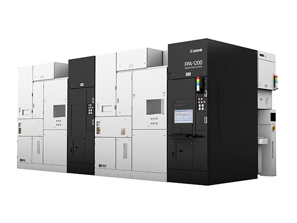
Canon's (TYO:7751) FPA-1200NZ2C, the most advanced production NIL tool, is a four-station cluster stepper specified at a 3.4 nanometer overlay, roughly 90 wafers per hour throughput, and sub-15 nanometer (down to about 10 nanometer) resolution using jet-and-flash imprint of a drop-dispensed resist against a physical template [17][18]. Its advantages are single-exposure fine patterning without projection optics and roughly 90 percent lower power. Its disqualifying weaknesses for logic are particle-driven defectivity, described as "quite high" by imec's Cedric Rolin, overlay stability across many layers, and template lifetime and replication economics [18][19]. imec's assessment is that NIL cannot match EUV quality for tightly packed logic at advanced nodes [19].
The NIL verdict: resolution-capable but defectivity- and overlay-limited; suited to 3D NAND, DRAM periphery, silicon photonics, power devices, and metalenses; structurally unsuitable for high-volume logic. Export availability is a second, likely decisive, constraint: Canon tooling falls within Japanese controls aligned with the US-Netherlands-Japan regime, and EE Times flags potential restrictions on sales to China, so FPA-1200NZ2C-class tools should be assumed not lawfully obtainable [19]. A Chinese startup claim of NIL-based photonic-chip production cutting costs 90 percent is a developer assertion in the photonics niche, not evidence for logic [24].
Domestic immersion DUV: a 28nm tool years from sub-10nm relevance.
The domestic effort centers on the Yuliangsheng/SMEE-derived SSA/800-class tool, reportedly assembled largely from domestic parts and undergoing trials at SMIC since September 2025 under the "Mount Everest" project [25]. Reported output is roughly five machines in 2026 and about twenty in 2027, delivered to SMIC, Hua Hong, and CXMT for production-line validation rather than volume [24]. The tool is specified for 28nm-class single-exposure patterning and, in principle, 7nm through multipatterning [23]. The skeptical analysis is that overlay is the gating parameter: ASML's overlay leadership rests on an installed base of hundreds to thousands of matched scanners studied over years, and a prototype with no install base cannot skip that incremental cycle [23]. SMEE's most advanced shipping product remains the SSA600-series 90nm-class dry ArF scanner, and a December 2024 single-source government contract specified a KrF scanner at 110 nanometer resolution and 15 nanometer overlay, a useful indicator of current production-grade capability [23]. The verdict: feasible at 28nm-class after validation, with realistic entry into SMIC's 28nm flow around 2027; overlay is asserted, not independently measured, and the leap to 16nm then 7nm-class production on domestic scanners is not expected before roughly 2030 [25]. It is a supply-security hedge against servicing cut-off of the ASML fleet, not a near-term capability expansion.
Domestic EUV: the source is not the constraint.
On sources, laser-induced discharge plasma (LDP), reportedly developed with Harbin Institute of Technology input and tested at a Huawei-associated facility in Shenzhen/Dongguan, evaporates and ionizes tin between electrodes to generate 13.5 nanometer light, reportedly reaching 100-150 watts in mid-2025 against a commercial requirement of at least 250 watts [13][11]. A December 2025 state-backed consortium reportedly certified a functional LDP prototype in Shenzhen, but the honest framing is that it generated EUV light and has not produced functional chips at commercial yield [11]. The more radical steady-state microbunching (SSMB) approach, a storage-ring accelerator concept from Tsinghua University with peer-reviewed theoretical foundations projecting kilowatt-level continuous output, has a dedicated facility reportedly begun at Xiong'an in early 2025, with commercial deployment placed beyond 2030 [12][11].
The decisive point is that the source is the most visible but not the binding subsystem. An integrated EUV scanner additionally requires Mo/Si multilayer projection optics at figure-and-finish tolerances that Zeiss alone has mastered and Changchun Institute of Optics trails; defect-free mask blanks, where Hoya and AGC (TYO:5201) are the only qualified suppliers and AGC has not demonstrated phase defectivity below 0.1 per square centimeter at actinic wavelength while Hoya has surpassed it on volume product, with a 5-7 year co-development cycle a new entrant cannot compress [40][41]; metal-oxide resists trading resolution against line-width roughness and sensitivity; and a pellicle with adequate EUV transmission and thermal survivability, absent which every mask particle prints as a killer defect [42][40]. The binding constraint is the mask-blank-and-pellicle-and-metrology layer, not the light. An analyst characterization places China's EUV at a stage similar to ASML in 2004, implying a decade-scale path [24].
The verdict: source work is genuine and advancing; an integrated, chip-producing, commercially viable domestic EUV tool is not achievable before roughly 2030 at the earliest and more plausibly beyond, with medium-to-low confidence, because the constraint is a supply-chain-wide co-development problem, not a single breakthrough, and because Hoya, AGC, and Zeiss supply is export-foreclosed, forcing domestic construction essentially from scratch.
The metrology, mask, resist, and pellicle dependency layer: the true bottleneck.
The hypothesis that metrology and inspection, not exposure, constitute the true chokepoint is substantially correct for the multipatterning path specifically. A SAQP-heavy flow is metrology-intensive in proportion to its pass count: every litho-etch cycle demands after-development and after-etch overlay and CD metrology, and edge-placement error, coupling overlay and CD across layers, becomes the governing yield metric at tight pitch [35][36]. The tools, optical and scatterometry-based overlay and CD metrology, high-voltage e-beam review with model-based physics algorithms, and actinic patterned-mask inspection, are dominated by KLA (NASDAQ:KLAC), with process-integrated metrology from Applied Materials (NASDAQ:AMAT), Lam Research (NASDAQ:LRCX), and Tokyo Electron (TYO:8035), and mask and optics metrology from Carl Zeiss SMT and Lasertec [35][36][42]. E-beam inspection at the required sensitivity is inherently low-throughput, forcing a sampling-versus-coverage trade that worsens as pass count rises. Domestic metrology and inspection is the ecosystem's thinnest layer, and the December 2024 BIS rules explicitly added node-agnostic tools, metrology among them, to the controlled list [37][39]. The judgment: metrology scaling does not keep pace with multipatterning demand, and this, as much as exposure, caps achievable yield.
 John D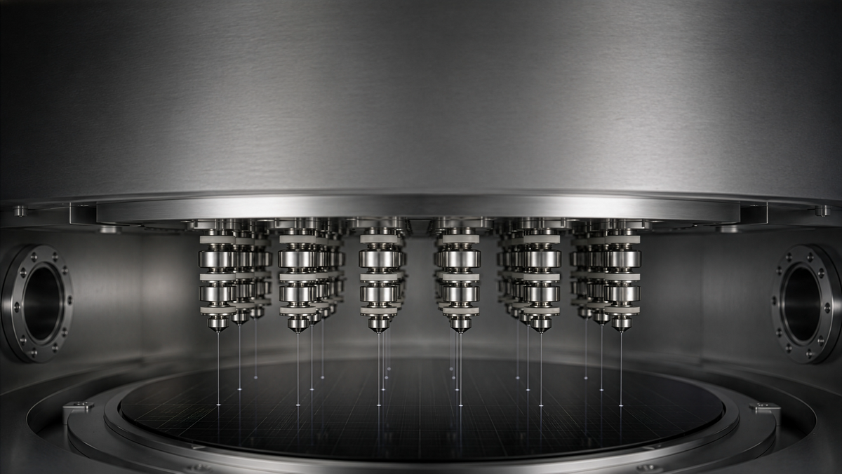
4. Device and Integration Assessment
Nanosheet GAA depends more on epitaxial superlattice growth, selective etch of sacrificial layers, and atomic-layer deposition of gate stacks than on a lithographic generation, drawing on exactly the etch and deposition capabilities where Naura and AMEC are strongest. SMIC is therefore likely able to introduce a nanosheet device on its immersion-plus-multipatterning base within the window, at the usual yield and density penalties. No independent teardown has yet established a shipping Chinese GAA logic product, so this is a feasibility assessment, not a demonstrated result.
CFET stacks n- and p-type devices vertically and is universally treated as a beyond-2nm, roughly A7/A5-node technology targeted for around 2031-2032 even by imec, TSMC, Intel, and Samsung [28][29]. imec's 2024 monolithic CFET demonstration achieved electrical functionality at 60 nanometer gate pitch with 50 nanometer n-to-p separation, and found that moving bottom-contact formation to the wafer backside raised top-device survival rate from 11 to 79 percent, underscoring how alignment- and litho-intensive the integration is [28]. TSMC's monolithic CFET inverter at 48 nanometer gate pitch remains a lab result its own engineers call years from fab integration [29]. As CFET's density payoff depends on precisely the tight-pitch lithography and overlay control China lacks, monolithic CFET at production scale is structurally blocked within the window. Sequential CFET, which bonds a second device tier via low-temperature layer transfer, is more accessible because it leans on bonding and CMP rather than a single ultra-tight litho step, and is the more plausible Chinese route, but it too is a post-2031 proposition for volume.
Backside power delivery (BSPDN) is the offset with the best evidence and the most favorable dependency profile, because nano-TSV formation, extreme wafer thinning, carrier bonding, and backside metallization draw on etch, deposition, bonding, and CMP, the domestic strengths, rather than on tight-pitch exposure. Intel's PowerVia on an Intel 4 test vehicle (Blue Sky Creek) demonstrated more than 30 percent platform-voltage-droop improvement, a 6 percent frequency benefit, and standard-cell utilization above 90 percent over large die areas, with Intel noting the 6 percent gain is about half a typical node's frequency benefit delivered with no transistor change [21][22]. imec's DTCO study found a BSPDN simultaneously delivering 6 percent frequency and 16 percent area improvement with no energy penalty versus a frontside network in high-density logic [20]. Intel relaxed its M0 pitch from 30 to 36 nanometers precisely because backside power freed the frontside stack, a relevant lesson that BSPDN can substitute for some pitch tightening [22]. The verdict: BSPDN is feasible on the domestic tool base, is worth on the order of half a node in frequency-or-area terms against published results, and is where China can most credibly close part of the gap; it does not by itself lift N6-class density to 5nm-class, and it adds thinning, bonding, and backside-metrology process risk.
The LogicFolding concept. On provenance, "LogicFolding" originates in a corporate conference disclosure, not a traceable patent. It was unveiled by He Tingbo, president of Huawei's semiconductor division and a board member, in a keynote titled "New Semiconductor Path in Practice" at the IEEE International Symposium on Circuits and Systems (ISCAS 2026) in Shanghai on May 25, 2026, alongside a "Tau (τ) Scaling Law," documented in Huawei's own press release [7][8][9]. No specific CNIPA or WIPO patent filing bearing the term "LogicFolding" was identified in this research; the term should be treated as a Huawei-coined architecture name announced in a keynote, with the underlying concept, folding planar logic into vertically stacked active tiers to shorten critical-path wiring, assessed on its technical merits. A supporting "true-3D" EDA prototype from Peking University's School of Integrated Circuits was disclosed two days later, reporting a 30 percent reduction in total internal wire length on open-source designs, again a prototype claim, not a production tool [43][44].
Huawei's own quantified claims, verbatim from its press release, are that over the past six years it has designed and mass-produced 381 chips based on the τ Scaling Law, and that by 2031 its high-end chips are expected to feature transistor density equivalent to 14-angstrom (1.4nm) processes; associated coverage adds a 55 percent transistor-density increase, a 41 percent power-efficiency gain, and about 13 percent higher clock frequency, with the first product being the Kirin 2026 in the Mate 90 series [7][8]. These are developer assertions that were not independently verified and that Huawei itself pairs with two acknowledged obstacles: inadequate EDA and, decisively, heat dissipation in stacked tiers [7][8][9]. Moor Insights' Anshel Sag noted that none of Huawei's prior "magical" breakthroughs have proven scalable [10]. The physically serious critique is the yield-compounding one: if each stacked tier yields around 50 percent, a two-tier folded die risks roughly a quarter usable, and SMIC's already-depressed 5nm-class yield compounds across layers [45]. The claimed "1.4nm-equivalent" density is a footprint-counting effect from stacking at unchanged etch pitch, not a lithographic equivalence [10].
The verdict: LogicFolding is best classified as a system-technology-co-optimization and packaging density-recovery program with an aspirational monolithic-3D-logic endpoint; its near-term embodiment (a fall-2026 Kirin) is a stacking-and-packaging play, and its data-center endpoint by 2030-2031 is thermally and yield-constrained and unproven. It is neither vaporware nor a validated node substitute.
Advanced packaging is where China can recover the most system-level performance per unit of lithographic deficit, and where it is closest to parity. Huawei's Ascend accelerators already use quad-chiplet designs; a Huawei patent describes bridge-style chiplet interconnect analogous to TSMC CoWoS-L or Intel EMIB-plus-Foveros rather than a monolithic interposer, with a reported total silicon area near 4,020 square millimeters across chiplets [43][54]. The substitution logic is sound: tying multiple N+2/N+3 chiplets together with high-bandwidth interconnect and HBM can approach the system performance of a single leading-edge die, and China's hybrid-bonding and TSV capability is comparatively strong [43][54]. The ceiling: packaging recovers throughput and integration density but not per-transistor energy efficiency, so a chiplet system built on N6-class silicon carries that silicon's power and area penalty, which is why the Kirin 9030 Pro performs like a three-year-old flagship and trails on efficiency by a wider margin than on raw performance [1]. Substitution stops working where energy-per-operation, not aggregate compute, is the binding constraint, precisely the AI-inference-at-scale and mobile-battery regimes.
5. Yield, Cost, and Capacity Modeling
Yield on a multipatterning flow can be framed with a Poisson or negative-binomial model in which die yield falls as exp(−D0·A) per critical layer and compounds multiplicatively across critical layers, where D0 is defect density and A is die area. For the Kirin 9030 at roughly 140 square millimeters with many SAQP-defined critical layers each carrying elevated D0 from added litho-etch cycles, the compounding drives composite yield well below single-layer figures; this is the mechanism, not a precise prediction, and public figures are ranges, not disclosures. The defensible range for N+3-class yield is roughly 30-50 percent, bracketed by the unverified 30 percent Korean trade estimate and TechInsights' "above 50 percent" N+2 judgment, trending downward as pitch tightens toward genuine 5nm-class [46][45][6]. Against a 15 percent N+1 baseline implying roughly 10x cost per good die versus TSMC 7nm, an improved N+3 plausibly runs 2-3x the merchant cost per good die, still prohibitive for price-sensitive markets but tolerable for state-procured product [47].
On capacity, the arithmetic that binds is scanner-hours per wafer. A SAQP-heavy flow consumes multiple immersion exposures per critical layer, so a wafer that would take a handful of EUV exposures at a comparable node instead consumes many immersion passes, each at finite throughput (an ASML NXT:1980Fi runs about 330 wafers per hour; the reported domestic tool far less) [27]. Multipatterning multiplies scanner-hours per wafer and, for a fixed fleet, divides achievable wafer starts, which is why capacity, not design, is the ceiling on Chinese leading-edge output [27]. Converting to annual good-die output: at 140 square millimeters, a 300-millimeter wafer yields on the order of 400 gross candidate die, so at 40 percent composite yield roughly 160 good die per wafer, and at 60,000 wafers per month a theoretical ceiling near 115 million good large-die per year before allocation, an upper bound that HBM supply and packaging throughput bind below.
For AI accelerators, HBM availability and packaging throughput bind before wafer capacity: CXMT targets HBM3 mass production by end-2026, reportedly dedicating around 20 percent of a roughly 300,000 wafers-per-month DRAM capacity to HBM, having shipped HBM3 samples on a 16 nanometer process in 8-high stacks to customers including Huawei in late 2025, with small-scale HBM3E reportedly beginning in 2026, though yield is flagged as low and these are partly anonymous-sourced reports [30][31][32]. Back-end stacking, bonding, warpage, and package-yield learning are the specific throughput constraints [30].

6. Application Mapping
The mapping must be read through the structural fact that cost tolerance differs by end market, converting an economically nonviable flow into a strategically acceptable one for the right customer.
High-performance AI logic for state and military procurement is the best fit for the SAQP-plus-chiplet-plus-domestic-HBM stack: a 2-3x cost penalty and 30-50 percent yield are acceptable when the buyer is the state, the alternative is no supply, and performance aggregates through packaging; this is the Ascend line's actual position [43][54]. General-purpose server CPUs (Kunpeng) sit in the same tolerant category.
Mobile SoCs for export are the worst fit: the Kirin 9030 Pro yields three-year-old flagship performance at a wide efficiency deficit, viable only in a protected domestic market willing to pay for sovereignty, not in open export competition [1][10]. DRAM and HBM are served by CXMT on DUV plus, plausibly, DSA for regular arrays, and are 3-4 years behind but structurally on-track [32]. 3D NAND (YMTC) is a vertical-scaling story largely decoupled from lithographic pitch and is China's most competitive advanced-memory segment. Silicon photonics, RF and analog, and power devices are well served by NIL (where obtainable), domestic immersion, and mature nodes, because their feature and defect budgets are forgiving; these are genuine near-term wins. Packaging and interposers are a domestic strength and the connective tissue of the whole strategy.
 John D
7. Economic and Market Dynamics
The economics are dominated by the subscription nature of leading-edge lithography. A scanner is a serviced asset requiring recalibration, replacement optics, source modules, and field engineering; ASML books this as installed-base management, which contributed 2.5 billion euros of 8.8 billion euros of first-quarter-2026 net sales (at a 53 percent gross margin and 2.8 billion euros net income) [27]. The strategic vulnerability of the Chinese fleet is therefore servicing and spare parts, which pending US legislation (the MATCH Act / H.R. 8170, reported out of committee April 22 with a Senate companion) would extend controls to cover, reaching installed tools, not just new exports [24]. Domestic tool substitution reached 35 percent of Chinese fab purchases by value in 2025, beating a 30 percent target, but that share is concentrated in etch and deposition; lithography, metrology, and inspection remain the import-dependent gaps [23][26]. Goldman projects domestic wafer-fab-equipment suppliers reaching 38 percent of the market by 2028, with lithography persistently excepted [26].
8. Regulatory and Export-Control Landscape
The controlling regime is the layered BIS rule set of October 2022, October 2023, April 2024, and the decisive December 2, 2024 package, which added controls on 24 types of semiconductor manufacturing equipment and 3 software tools, imposed China-wide HBM controls (capturing HBM2 and above by bandwidth density), created two new Foreign Direct Product rules, and added 140 entities including SMIC affiliates under Footnote 5 designations effective December 31, 2024 [37][38]. The 2024 rules explicitly reached node-agnostic tools and DUV multipatterning techniques, and extended to South Korean firms operating in China [39]. The most consequential single fact is that EUV has been foreclosed entirely, never shipped to China, which BIS and allied analysis identify as the most effective restriction, while ASML immersion DUV has continued to reach China through allowed channels and secondary markets, sustaining the installed base the whole SAQP strategy depends on [39]. A countervailing 2025 development is the December 8, 2025 decision, implemented by BIS rule, allowing case-by-case licensing of Nvidia H200 and AMD MI325X-class accelerators to approved Chinese customers, which relieves near-term AI-compute pressure and marginally reduces the forcing function behind domestic accelerators [48]. The Dutch and Japanese controls align with the US regime on advanced DUV, EUV, and, relevantly for NIL, Canon tooling [24][19].
9. Geopolitical and Strategic Dimensions
China is funding a parallel, sovereignty-first ecosystem in which profitability is subordinated to existence at the leading edge, and in which state procurement absorbs the cost and yield penalties that would kill a commercial flow [27]. State mandates that state-funded data centers use domestic chips, and the reported optimization of major Chinese AI models for Huawei silicon, create a captive demand floor that makes the economics viable [44]. The reciprocal Western leverage is servicing, spare parts, and the mask-blank/pellicle/optics/metrology bottlenecks, more durable than the exposure-tool bottleneck because they are supply-chain-wide co-development problems. Chinese retaliation through gallium, germanium, antimony, and graphite export restrictions is the counter-leverage [38].
 John D
10. Structural Blockages Versus Resource-and-Time Constraints, and Falsification Tripwires
Structurally blocked within the 2026-2031 window, not clearable by money and time alone at that horizon: an integrated, commercially viable domestic EUV tool (blocked by the mask-blank, pellicle, optics, and actinic-inspection co-development cycle, not the source); monolithic CFET at production scale (blocked by tight-pitch litho and overlay dependence); genuine 2nm-class single-die logic at commercial cost and volume (blocked by the compound of the above).
Merely difficult, and clearable by sustained state investment: domestic 28nm-class immersion (on track for roughly 2027, sub-10nm not before roughly 2030); nanosheet GAA on the immersion base; backside power delivery; HBM3/HBM3E; sequential CFET on a longer horizon.
Confined by physics to non-logic regardless of investment: DSA for random logic; NIL for high-volume logic.
The falsification tripwires, each concrete and dated: the judgment that China cannot field high-volume EUV before 2030 would be overturned by a TechInsights or SemiAnalysis teardown, before end-2028, of a Chinese logic product exhibiting EUV-characteristic single-exposure pitch below 30 nanometers with no multipatterning signature, or by a credibly disclosed domestic EUV source sustained above 250 watts integrated into a scanner printing device wafers at yield. The judgment that domestic immersion cannot reach sub-10nm before roughly 2030 would fall on a disclosed SSA-class tool achieving sub-3-nanometer overlay in a qualified production flow before end-2027. The judgment that SMIC leading-edge yield sits at 30-50 percent would be revised by an SMIC capacity or yield disclosure, or a teardown-inferred yield, materially outside that band. The judgment that CFET is blocked would fall on a Chinese conference presentation (IEDM, VLSI, or ISSCC) showing a functional CFET inverter at sub-60-nanometer gate pitch on a domestic line before 2029. The judgment on LogicFolding would be overturned by a teardown of a fall-2026 or 2027 Kirin confirming genuine monolithic stacked-active-logic tiers (not package-level stacking) at disclosed density and acceptable yield. The judgment that domestic HBM binds AI output would be revised by a CXMT HBM3E volume-and-yield disclosure matching merchant benchmarks before end-2027.
11. Risk Matrix
| Risk | Likelihood | Impact | Mitigations |
|---|---|---|---|
| ASML servicing/spares cut-off (MATCH Act) degrades installed immersion fleet | Medium | High | Stockpiling spares; domestic servicing capability; accelerate SSA-class qualification |
| SMIC 5nm-class yield stalls below 30%, starving Ascend supply | Medium-High | High | Chiplet partitioning to smaller die; DTCO; state absorption of cost; military allocation priority |
| Domestic HBM (CXMT) yield/volume shortfall binds AI accelerators | High | High | H200/MI325X licensed imports as bridge; YMTC/XMC packaging capacity; third-party import |
| Domestic EUV proves further off than 2030 | High | Medium | Deepen SAQP/BSPDN roadmap; SSMB as long-horizon leapfrog; accept multi-node deficit |
| Metrology/inspection cannot scale with multipatterning pass count | High | High | KLA-class acquisition via secondary channels; domestic e-beam investment; sampling optimization |
| Overlay on domestic scanners fails to reach production spec | Medium-High | Medium | Retain ASML tools for critical layers; hybrid domestic/ASML flow; extended qualification |
| LogicFolding thermal/yield failure at data-center scale | Medium-High | Medium | Fall back to chiplet-plus-HBM packaging; limit stacking to mobile; STCO |
| Western relaxation (H200 licensing) undercuts domestic-accelerator demand floor | Medium | Low-Medium | State procurement mandates; sovereignty framing; dual-source |
| Further BIS tightening reaches mature-node and node-agnostic tools | Medium | Medium | Accelerate domestic etch/deposition/CMP (already strong); inventory |
12. Scenarios to 2031
Three scenarios with explicitly subjective probabilities summing to unity, reflecting reasoning from current evidence, not calculated frequencies.
Scenario A, "Grinding Ascent" (approximately 55 percent). SMIC pushes SAQP to a genuine 5nm-class-density node (CGP near 51 nanometers, roughly 137 MTr/mm²) by roughly 2028-2029 at 30-45 percent yield and 2-3x merchant cost, adds nanosheet GAA and backside power for a further half-node of effective gain, and relies on chiplet packaging and CXMT HBM3E for AI systems. Domestic 28nm immersion qualifies around 2027; EUV remains pre-production. China fields competitive state-and-military AI logic at high cost and constrained volume, remains uncompetitive in export mobile, and stays roughly one-and-a-half to two nodes behind the merchant leading edge on efficiency. This is the trajectory the current evidence most supports.
Scenario B, "Bottleneck Bites" (approximately 30 percent). MATCH Act servicing restrictions degrade the ASML fleet faster than domestic tools mature, metrology fails to scale with pass count, and HBM yield stalls; SMIC yield stays near 30 percent, output is rationed to military priorities, and the effective deficit widens. LogicFolding underdelivers thermally. China's leading-edge program persists but as a strategic reserve, not a competitive industry.
Scenario C, "Leapfrog Surprise" (approximately 15 percent). One structural constraint clears earlier than expected, most plausibly a domestic immersion overlay breakthrough or an unexpectedly rapid mask-blank/pellicle solution enabling limited EUV insertion on critical layers by around 2029-2030, or an SSMB source maturing faster than its beyond-2030 consensus. This would compress the timeline by a node and is the tail the Section 10 tripwires are designed to detect.
Recommendations
For institutional investors, the actionable reading is that ASML's immersion-plus-servicing franchise and the KLA/Applied/Lam/Tokyo Electron/Zeiss metrology-and-optics complex are the durable bottlenecks and higher-conviction long positions, because the Chinese program deepens rather than reduces dependence on immersion exposure and metrology through 2031, and because installed-base management is the sticky, defensible revenue line [27][40]. Hoya and AGC mask-blank scarcity is an under-appreciated structural moat [40]. Treat Chinese "5nm/1.4nm" and LogicFolding headlines as marketing generations, not physical capability, and underwrite Chinese leading-edge names on state-demand-floor logic and packaging/memory execution rather than on node parity. The staged benchmark that would change the thesis is a teardown showing sub-30-nanometer single-exposure pitch, or a CXMT HBM3E yield disclosure at merchant parity, before end-2027.
For export-control policymakers, the evidence supports a sharp reprioritization. The exposure-tool control (EUV foreclosure) has worked, but the highest-leverage, most durable controls are on the mask-blank, pellicle, precision-optics, actinic-mask-inspection, and metrology-and-inspection layers, and on servicing and spare parts for the installed immersion fleet, because these are supply-chain-wide co-development problems China cannot brute-force on a five-year horizon [40][42][24]. The MATCH Act's extension to servicing is therefore the single highest-impact available measure. Policymakers should weigh that the H200/MI325X licensing relaxation reduces the demand-side forcing function behind indigenous accelerators, a genuine trade-off between near-term commercial access and long-term indigenization incentives [48]. The metric that should trigger tightening is any teardown or disclosure indicating domestic metrology or mask-blank capability crossing into production qualification.
For incumbent equipment and materials suppliers (treated briefly), expect sustained but plateauing Chinese immersion, etch, and deposition demand, aggressive domestic substitution in etch/deposition/CMP specifically, and durable dependence in litho, metrology, mask blanks, and optics; protect the latter and price the servicing franchise accordingly.
Caveats
The dominant caveat is source contamination: much of the Chinese advanced-node record consists of state-media claims, single-analyst social-media reports (the "5nm without EUV" claim traces to analyst William Huo on X), anonymous trade-press sourcing, and forward-looking roadmap projections presented as achievements; these have been flagged as claims requiring corroboration rather than treated as evidence [5][12]. The highest-quality evidence, TechInsights and SemiAnalysis teardowns, is partly paywalled, and the two firms are commercial competitors, with SemiAnalysis openly criticizing TechInsights; their N+3 figures are nonetheless internally consistent and mutually corroborating on the key parameters, and TechInsights' specific critical-dimension measurements for N+3 were found but never publicly released [1]. Yield figures for SMIC are estimates, not disclosures, and range widely. Capacity figures blend disclosures with Goldman and analyst models. Huawei's LogicFolding and τ-scaling density and efficiency figures are unverified developer assertions. EUV source-power and prototype-certification reports rest substantially on Chinese and secondary reporting. The evidence cutoff is September 3, 2026, and several threads (the fall-2026 Kirin, CXMT HBM3E ramp, MATCH Act passage, domestic scanner qualification) will resolve shortly after and should be re-checked against the Section 10 tripwires.

References
[1] SemiAnalysis STEEL Team. 2026. "Is SMIC N+3's Metal Pitch Smaller than Intel 18A's?" SemiAnalysis, June 14.
[5] Tom's Hardware. 2026. "SMIC and Huawei could use quadruple patterning for China-made 5nm chips."
[6] SemiWiki. 2026. "SMIC BEOL Photolithography Process Analysis / N+3 Yield Issues."
[7] Huawei. 2026. "HUAWEI Presents the Tau (τ) Scaling Law, Enabling Breakthroughs in Transistor Density and System Performance." Huawei Newsroom, May 25.
[8] Tom's Hardware. 2026. "Huawei claims sanctions-busting breakthrough with 1.4nm-class chips by 2031."
[9] Quartz. 2026. "Huawei LogicFolding chip design aims to match 1.4nm by 2031." May 26.
[10] Richard's Gadgets (Substack). 2026. "Huawei's 'LogicFolding' chip tech aims to close the gap amid US sanctions."
[11] EE Times. 2026. "China EUV Breakthrough and the Rise of the 'Silicon Curtain.'"
[12] Jiang, B., C. Feng, C. Li, et al. 2022. "A synchrotron-based kilowatt-level radiation source for EUV lithography." Scientific Reports 12: 3325 (arXiv 2110.08987).
[13] Global SMT & Packaging Asia. 2025. "China's EUV breakthrough: Huawei, SMIC reportedly advancing LDP lithography."
[14] Stanford Digital Repository. "Block Copolymer Directed Self-Assembly for Patterning Memory and Logic."
[15] Journal of Vacuum Science & Technology B. 2020. "Block copolymer directed self-assembly defect modes induced by localized errors in chemoepitaxial guiding underlayers." 38(3): 032604 (AIP).
[16] International Journal of Extreme Manufacturing (IOPscience). 2020. "Directed self-assembly of block copolymers for sub-10 nm fabrication."
[17] Canon Global. "FPA-1200NZ2C." Product page.
[18] Semiconductor Engineering. "What Happened To Nanoimprint Litho?"
[19] EE Times. "Canon Litho Tool Years From Commercial Use, Analysts Say."
[20] imec. "DTCO Study of Backside Power Delivery Options."
[21] Hafez, W., et al. 2023. "Intel PowerVia Technology: Backside Power Delivery for High Density and High-Performance Computing." IEEE Symposium on VLSI Technology and Circuits, Kyoto.
[22] Intel Newsroom. 2023. "PowerVia Test Shows Industry-Leading Performance." June 5; IEEE Spectrum, "Intel Is All-In on Backside Power Delivery."
[23] Tom's Hardware. 2026. "Chinese chipmaking tool roadmaps examined."
[24] Tom's Hardware. 2026. "China's EUV technology 'at a similar stage to ASML in 2004,' analyst claims"; and related Tom's Hardware reporting on domestic immersion and MATCH Act.
[25] TechPowerUp. 2026. "SMIC Begins Trials of China's First Homegrown Immersion DUV Scanner."
[26] South China Morning Post / Interesting Engineering. 2026. "China could sharply narrow advanced chip supply gap by 2035" (Goldman Sachs model).
[27] Vested Finance. 2026. "Is China Building Chip Machines That Threaten ASML?"; ASML Q1 2026 results (April 15, 2026).
[28] imec. 2024. "Monolithic CFET Devices with Stacked Bottom and Top Contacts." VLSI 2024.
[29] eeNews Europe. 2024. "IEDM: CFETs make progress at 5nm and 7angstrom."
[30] Tom's Hardware. 2026. "Chinese semiconductor industry gears up for domestic HBM3 production by the end of 2026."
[31] TechPowerUp. 2026. "CXMT Reportedly Plans to Dedicate 20% of Mass Production Capacity to HBM3 Line in 2026."
[32] ChinaTalk. "Mapping China's HBM Advances"; Cryptobriefing, "CXMT develops HBM3 memory chips."
[33] Angstronomics. "The TRUTH of TSMC 5nm."
[34] WikiChip Fuse. "TSMC Details 5 nm"; SemiWiki, "SRAM Scaling Isn't Dead After All — TSMC's 2nm."
[35] Semiconductor Engineering. "Overlay Challenges On The Rise."
[36] SPIE. 2025. Metrology, Inspection, and Process Control XXXIX (KLA ePhysX e-beam overlay).
[37] Bureau of Industry and Security. 2024. "Commerce Strengthens Export Controls to Restrict China's Capability to Produce Advanced Semiconductors." December 2.
[38] Holland & Knight; Alston & Bird; Covington & Burling. 2024. Client advisories on the December 2, 2024 BIS rules.
[39] Congressional Research Service. CRS Report R48642, "U.S. Export Controls and China: Advanced Semiconductors."
[40] Almansour, K. (Substack). "On Mask Blanks and the Substrate Sovereigns of Advanced Lithography"; SemiconductorX, "EUV Mask Blanks & Pellicles."
[41] Semiconductor Engineering. "EUV Mask Blank Battle Brewing."
[42] Averroes. "EUV Defect Detection: Challenges and AI Solutions."
[43] Tom's Hardware / TrendForce. 2025. "Patent reveals Huawei's quad-chiplet rival for Nvidia's Rubin AI GPUs."
[44] Tom's Hardware; Digitimes; South China Morning Post. 2026. "Peking University builds 3D chip design tool tailored to Huawei's LogicFolding."
[45] The National Interest. 2026. "Huawei Can't Shrink Its Chips, So It's Folding Them."
[46] SemiWiki. "Kirin 9000s Analysis" (Dan Hutcheson / TechInsights on N+2 yield above 50 percent).
[47] Mulvenon, J. 2023. "SMIC Races Over BIS Speed Bump to Fulfill China's Strategic Ambitions."
[48] Bureau of Industry and Security. 2025. "License Review Policy for Semiconductors Exported to China" (H200/MI325X, December 8).
[54] TrendForce. 2025. "Huawei's Quad-Chiplet 910D Reportedly Takes Shape with Advanced Packaging."