Multi-Column Electron-Beam Lithography: Why E-Beam Direct Write Cannot Replace EUV
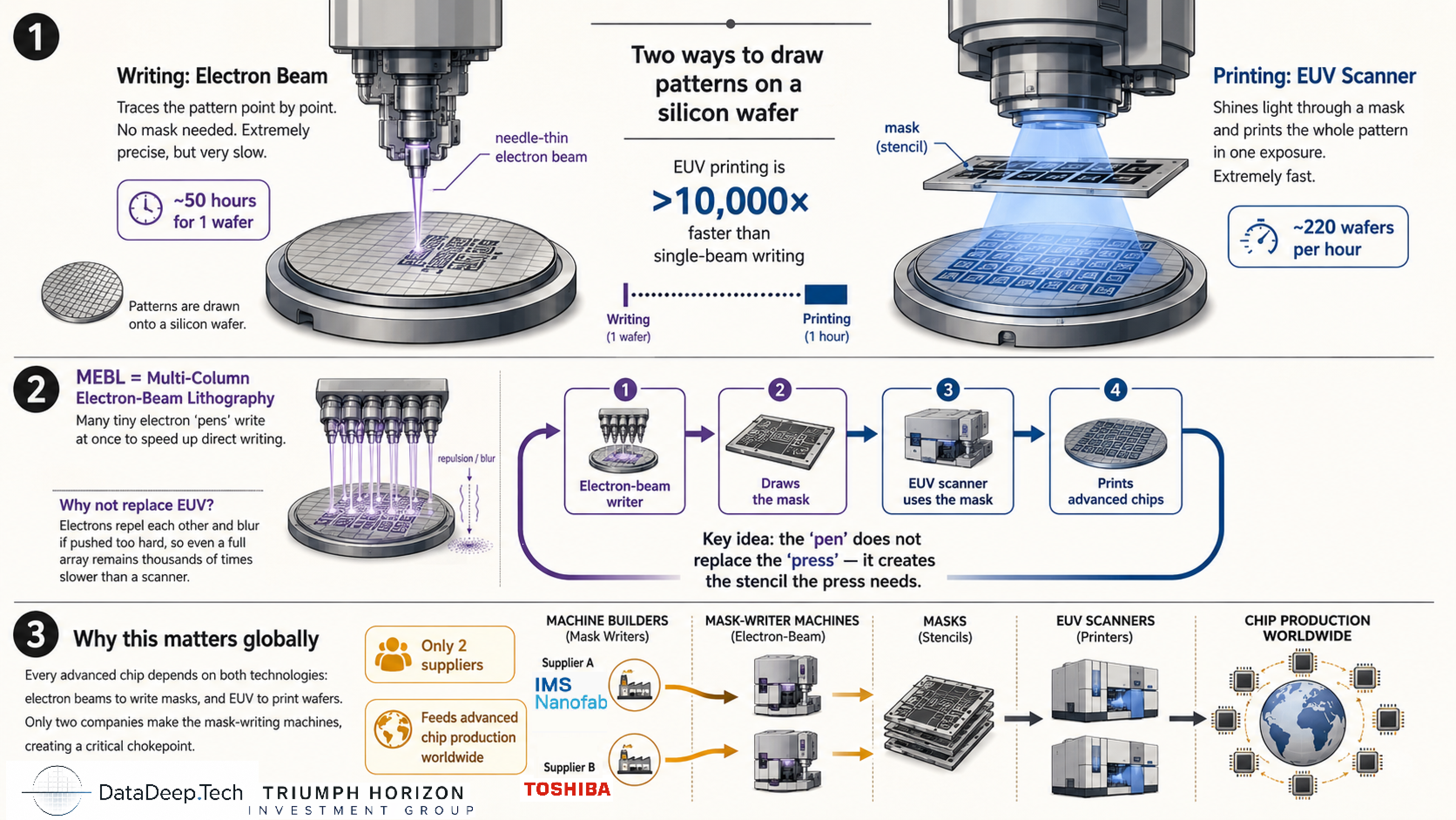
A single e-beam column writes one 300mm wafer in 50 to 60 hours. An EUV scanner does 220 an hour. The four-order gap defines where maskless wins.

1. Summary
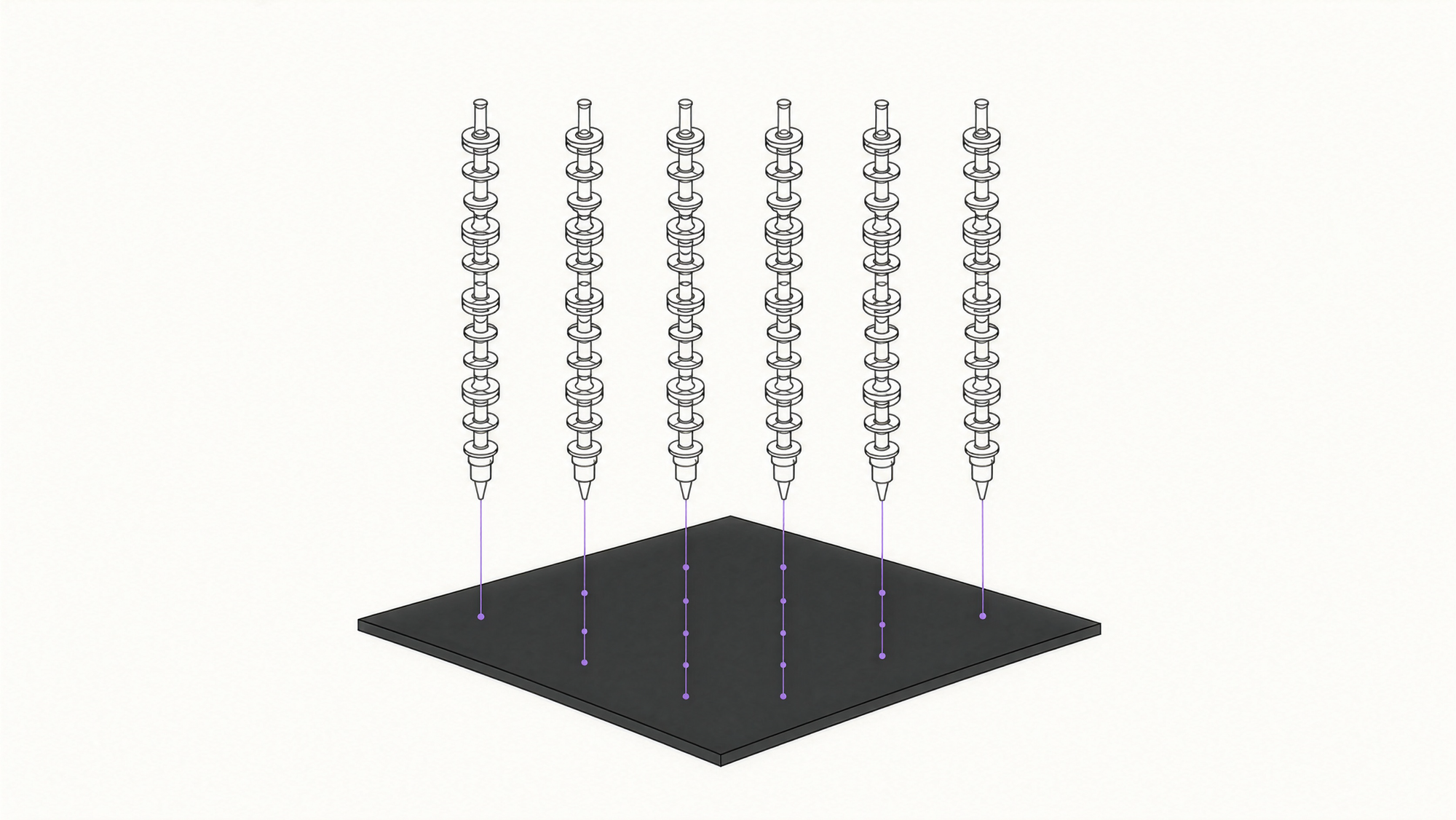
Multi-column electron-beam lithography (MEBL) is a maskless patterning architecture that parallelizes electron-beam writing by deploying an array of independent miniature electron-optical columns, each with its own source, optics, deflection, and control. It is distinct from single-column multi-beam systems, which split one electron source into thousands or hundreds of thousands of beamlets through an aperture plate or a micro-electro-mechanical-systems (MEMS) blanker array. The two are routinely conflated in trade coverage; the distinction is central to this report.
The central finding is that column-level parallelization does not overturn the fundamental economics of electron-beam lithography for high-volume manufacturing (HVM), but it has found commercial niches. Serial single-column direct write has never reached HVM because the physics of charged particles caps the usable current in a single column: Coulomb interactions between electrons blur the beam as current rises, so a single column takes on the order of 50 to 60 hours to write one 300mm wafer at advanced nodes [1], against 220 wafers per hour for a state-of-the-art extreme ultraviolet (EUV) scanner [2]. That is a per-tool throughput gap of roughly four orders of magnitude.
Conclusions: First, the one unambiguous commercial success of parallel electron optics in lithography is mask writing, not wafer writing: IMS Nanofabrication and NuFlare Technology multi-beam mask writers are now the industry-standard tools for advanced and EUV photomasks, a market on the order of USD 0.8 to 1 billion [3]. Second, for direct wafer writing, the opportunity is low-volume, high-mix niches: advanced-packaging redistribution and interposers, secure chip identification, photonics and quantum-device prototyping, and rapid prototyping. Multibeam Corporation is the last independent multi-column direct-write company standing after the collapse of Mapper Lithography (2018) and KLA's exit from its reflective electron-beam lithography (REBL) program. Third, the recurring narrative that e-beam lithography gives China a workaround to EUV denial does not survive quantitative scrutiny: at demonstrated throughputs, a maskless e-beam route cannot sustain the wafer output of even a single EUV scanner, let alone a fab [4].
Multi-Column Electron-Beam Lithography: Physics, Players, Economics, and Strategic Significance
2. Contextual and Scientific Background
2.1 The fundamental throughput problem
Electron-beam lithography can resolve features far smaller than the wavelength limits that constrain optical systems; for practical purposes its ultimate resolution is not the binding constraint. The binding constraint is throughput. In a probe-forming (focused-beam) system, all of the writing current must pass through a small aperture and be focused to a fine spot. As beam current rises, stochastic Coulomb interactions between electrons, comprising space-charge defocus, the Boersch effect (energy spread feeding chromatic aberration), and stochastic trajectory displacement, blur the spot and destroy resolution [5]. This is the physical mechanism that has capped single-column throughput for four decades.
The severity is quantifiable. Analyses of the current-blur tradeoff find that image blur from Coulomb interactions scales roughly as beam current to the power 0.6 to 0.9 and inversely with numerical aperture; higher acceleration voltage reduces blur (approximately as voltage to the negative 1.6 power) but raises proximity effects and cost [6]. The net result is that a single variable-shaped-beam (VSB) column writing a critical layer at the 65nm node can require on the order of 10^11 shots per 300mm wafer, roughly 50 to 60 hours of write time per wafer [1]. Patents in the field describe the general range as 10 to 100 hours to write an entire wafer [7]. Either way, a single column delivers on the order of 0.02 wafers per hour.
A second, independent constraint is the resist-sensitivity-versus-shot-noise tradeoff. To pattern a feature reliably, enough electrons must be deposited per pixel to average out Poisson shot noise. A representative figure: achieving 5 percent (3-sigma) dose control at a 45nm pixel requires roughly 4,000 electrons per pixel, corresponding to a dose of about 30 microcoulombs per square centimeter [8]. More sensitive resists need fewer electrons and write faster but suffer worse shot-noise-driven line-edge roughness; less sensitive resists give better fidelity but demand more dose and therefore more time. This tradeoff means throughput cannot be bought simply by making resist faster.
2.2 Two philosophies of parallelization
There are two ways to beat the single-column current limit, and they are physically distinct.
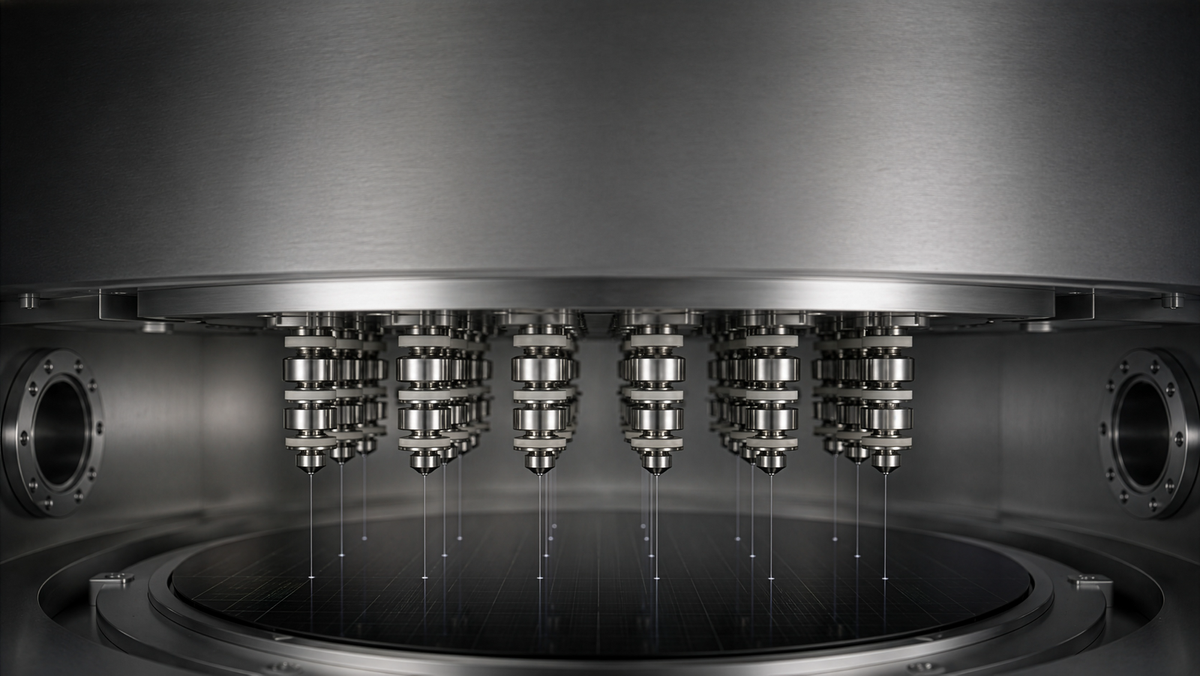
The many-columns philosophy (true multi-column, the core subject) places an array of complete, miniaturized columns side by side, each with its own source and optics, each writing a different region of the wafer simultaneously. Due to the total current being distributed across many spatially separated columns, no single aperture carries the full load, and Coulomb blur within each column stays low. Advantest's (ATEYY) multi-column cell work made this explicit: "Coulomb interaction between beams of different [column cells] no more exists and parallel writing is carried out" [9]. The engineering burden shifts to miniaturization, column-to-column matching, and stitching the regions together seamlessly.
The many-beamlets philosophy (single-column multi-beam) takes one broad electron source and splits it into thousands to hundreds of thousands of beamlets using an aperture plate, then switches each beamlet on or off with a MEMS blanker array, demagnifying the whole array onto the target through shared optics. This is the architecture of IMS Nanofabrication and NuFlare mask writers and of the defunct Mapper direct-write tool [10][11]. Its structural advantage is that a single, well-corrected optical column can be manufactured to extreme precision and shared across a very large beamlet count, and write time becomes independent of pattern complexity because the pattern is rasterized to a fixed pixel grid [10].
Each philosophy holds an advantage in a different regime. Single-column multi-beam scales beamlet count enormously within one precision column, which is why it won in mask writing, where the target is a single small reticle and shared optics can be lavished with correction. Many-columns scales the addressable area, in principle allowing coverage of a full 300mm wafer and very large depth of focus, which is why it is the more natural fit for full-wafer direct write, advanced packaging over topography, and large-format die [12]. The distinction matters commercially: the demonstrated winners in mask writing are beamlet-parallel; the surviving direct-write contender, Multibeam, is column-parallel.

2.3 Historical precedent: why e-beam HVM ambitions have repeatedly collapsed
The current generation is not the first attempt. In the 1970s IBM pioneered shaped-beam direct write and ran it profitably in quick-turnaround-time facilities, but shaped beams could not keep pace with Moore's Law because of the Coulomb limit [5]. In the 1990s two electron projection lithography (EPL) programs, Bell Labs' SCALPEL (Scattering with Angular Limitation in Projection Electron-beam Lithography) and IBM's PREVAIL (Projection Reduction Exposure with Variable Axis Immersion Lenses, developed with Nikon), attempted to emulate optical steppers by projecting a mask image with electrons. Nikon shipped a PREVAIL-based stepper to Selete in 2003 [5]. Both were ultimately abandoned: projection e-beam throughput was limited by the combined effects of field curvature in the projection lenses and Coulomb interaction in the beam, described in the literature as fundamental physical limitations with little scope for improvement, and the market chose optical and then EUV [13]. This history is a base rate against which new e-beam HVM claim could be assessed.
```html id="stock-chart-code"
3. Key Players and Stakeholders
3.1 Multi-column direct write (core subject)
Multibeam Corporation (Santa Clara, California; privately held) is the central player in true multi-column direct write. Founded in 2010 by Dr. David K. Lam, founder and first CEO of Lam Research (NASDAQ: LRCX), the company acquired proprietary e-beam technology and developed an all-electrostatic miniature column array [14]. Its MEBL platform uses a 5 kV beam energy, is available in 150mm, 200mm and 300mm configurations, and quotes a throughput of 2 to 25 wafers per hour per writing module with greater than 100 micron depth of focus (vendor-asserted) [15]. It is modular: modules can be added for higher throughput. Data preparation is integrated with Synopsys (NASDAQ: SNPS) software [16]. Multibeam shipped its first system to SkyWater Technology (NASDAQ: SKYT) in Bloomington, Minnesota in July 2024; SkyWater is a US-based, DMEA-accredited Trusted Supplier, and the stated use cases are early prototyping, secure chip ID for anti-counterfeit applications, full-wafer patterning for focal-plane read-out ICs and large-format die, MEMS, and photonics [17]. Investors include Onto Innovation (NYSE: ONTO), Lam Capital, UMC Capital and MediaTek Capital [15]. Multibeam holds a patent portfolio it describes as 46 awarded US patents [18]. The company's stated application targets are Complementary E-Beam Lithography (CEBL, patterning cuts and vias in conjunction with optical lithography), Secure Chip ID, advanced-packaging interposers, and photonics [14].
 Semiecosystem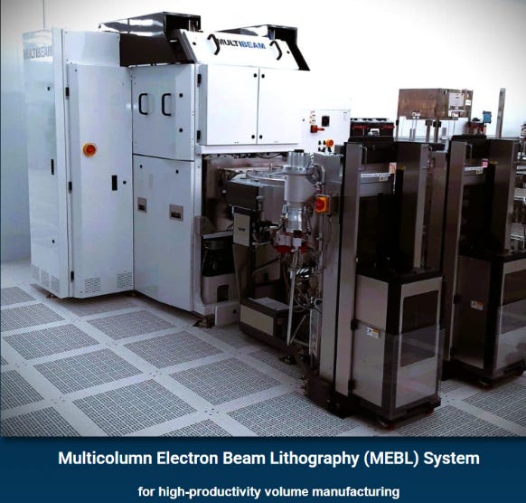
The demonstrated-versus-asserted distinction matters here. The shipment to SkyWater and the physical existence of the tool are documented. The throughput figure of 2 to 25 wafers per hour per module, the claim of being "orders of magnitude faster" than conventional e-beam tools, and Lam's statement that Multibeam could make certain fabrication steps "100 times more productive" are vendor assertions [15][17][19]; no peer-reviewed tool-performance data with independently verified throughput at a specified node and dose was identified in this research.
Advantest (TYO:6857) developed the multi-column cell (MCC) architecture, arguably the most literal realization of many-columns for cell-projection mask and wafer writing. Advantest's MCC used arrays of 4 or 16 column cells, each combining VSB and character projection, with a "lotus root lens," to expose a mask four to sixteen times faster than a single column [9]. The direct-write extension, MCC8, targeted 5 wafers per hour with 8 column cells and more than 30 wafers per hour by clustering six MCC8 units [20]. A more aggressive study set a target of 100 wafers per hour at the 14nm node using 150 beams, 10 clusters, 100 giga-shots per wafer, 250 A/cm2 and 75 microcoulombs per square centimeter [21]. Crucially, MCC8 never reached production: only a four-column-cell proof-of-concept (MCCPOC) was built, in March 2010, under Japan's ASET Mask-D2I program funded by NEDO, demonstrating mix-and-match overlay better than 5nm [20][22]. Advantest's last commercial EB lithography system was the F7000 direct-write tool (installed at imec in 2015, an R&D and small-lot tool), and the company today holds only a niche R&D position, having ceded leading-edge mask writing to NuFlare, IMS and JEOL [3].
Academic and national-laboratory multi-column work traces to IBM's T.J. Watson Research Center, where T.H.P. Chang and colleagues developed scanning-tunneling-microscope-aligned miniature electron-beam columns ("microcolumns") roughly 3.5mm long, demonstrating a 10nm probe at about 1 nA and 1 keV [23]. Chang's 1992 paper projected that with 10 columns per 20mm x 20mm chip, throughput of fifty 200mm wafers per hour or more might be achievable at 100nm line width (disputed on physical grounds in subsequent patent literature) [24]. Proof-of-concept arrayed microcolumn operation and a 20mm x 20mm footprint microcolumn were demonstrated in the 1990s [25]. This line of work is the intellectual ancestor of both Multibeam and the broader miniaturized-column field, but it never left the laboratory as a lithography product.
3.2 Single-column multi-beam mask writers (competitive context)
IMS Nanofabrication (Vienna, Austria) is the dominant force in multi-beam mask writing. Its Multi-Beam Mask Writer (MBMW) uses a multi-beam column providing 262,000 programmable beams of 20nm beam size, current density adjustable to 1 A/cm2 for total beam current up to 1 microamp, and (with the upgraded 120 Gbit/s data path introduced in 2016) can print full-field 7nm-node layouts in under 10 hours [26]. The first proof-of-concept tool was realized in 2012; the MBMW-101 first generation entered the market in 2016 for the 7nm node; the MBMW-201 second generation entered in Q1 2019 for the 5nm node; the MBMW-301 targets nodes down to 2nm and below and high-numerical-aperture EUV requirements [10][27]. The MBMW-100 Flex targets mature and intermediate nodes (32nm to 10nm) and reduces mask write time to 7 to 12 hours [27][28]. IMS multi-beam writers are the enabling tool for curvilinear inverse lithography technology (ILT) masks, because write time is independent of pattern complexity: any set of shapes rasterizes to a fixed pixel grid, so complex curvilinear ILT costs no extra write time [10]. This is the decisive advantage over the preceding single VSB technology.
IMS ownership structure carries strategic weight. Intel (NASDAQ: INTC) first invested in 2009 and acquired IMS fully in 2015. In June 2023 Intel agreed to sell an approximately 20 percent stake to Bain Capital Special Situations for USD 860 million, and in September 2023 a further approximately 10 percent to TSMC (NYSE: TSM) for about USD 430 million, both at a valuation of roughly USD 4.3 billion; Intel reported combined net proceeds of about USD 1.4 billion for the 32 percent sold [29][30]. Intel retains majority ownership; IMS operates as a standalone subsidiary under CEO Dr. Elmar Platzgummer [29]. The cap table is remarkable: the world's leading mask-writer maker is majority-owned by Intel with a minority stake held by Intel's principal foundry rival TSMC, plus a financial sponsor. IMS held a revenue share reported at 81.52 percent of the multi-beam mask-writer market in 2024 [3].
NuFlare Technology (Yokohama, Japan; a Toshiba group company) is the principal competitor. Its MBM-1000, developed from 2012 and targeted at the 5nm node, uses a 512 x 512 array of 10nm beamlets on a 32 micron pitch, a blanking aperture array, single 50 kV acceleration, 500 nA total current at 2 A/cm2 current density, and a data path designed for 300 Gbit/s [11]. The latest MBM-2000PLUS achieves a write time of 8.7 hours over a 104mm x 130mm area for a 150 microcoulomb per square centimeter resist, with global position accuracy of 1.2nm, local position accuracy of 0.5nm and local critical dimension uniformity of 0.61nm, using a beam current density of 3.2 A/cm2 [11]. NuFlare also remains the leading supplier of the preceding VSB mask writers (EBM series), giving it an installed base and a migration path [11].
Mapper Lithography (Delft, Netherlands; defunct) is the most instructive failure. Founded in 2000 as a spinoff of Delft University of Technology, Mapper pursued a MEMS-blanker massively parallel direct-write architecture. Its design target was 13,000-plus electron beams (13,260 beams delivering 170 microamps to the wafer, each beam split into 49 sub-beams) for a throughput exceeding 10 wafers per hour at the 22nm node [31]. The physics gap was severe: a dispenser cathode realistically delivered about 0.3 nA per beam at 25nm spot size, nearly a factor of 50 below the 13 nA per beam required for 10 wafers per hour, which is why the 49-sub-beam scheme was necessary [32]. In practice the pre-production Matrix 1.1 tool at CEA-Leti had 1,300 beams with only about half operational and reached 42nm half-pitch. After almost 20 years and no production-grade tool, investors withdrew and Mapper was declared bankrupt on 28 December 2018 [33]. ASML (NASDAQ: ASML) acquired the intellectual-property assets in January 2019 (a figure later reported at about EUR 75 million, or USD 79 million) and offered positions to Mapper R&D and assembly staff, folding them into its e-beam metrology and inspection business, not lithography [34][35]. ASML stated it would not continue developing Mapper's lithography technology, having concluded around 2000 that e-beam would never meet throughput requirements [36]. Notably, a Dutch press reconstruction reported that the Pentagon urged the Dutch government to intervene to keep Mapper's assets out of Chinese hands after Mapper had reached out to potential Chinese investors, and ASML CEO Peter Wennink characterized the maskless-unique-IC market as "one tool a year at most" [36].
KLA (NASDAQ: KLAC), REBL, and DARPA provide further failure-mode evidence. KLA-Tencor's Reflective Electron Beam Lithography (REBL) program, funded under DARPA's Maskless Nanowriter program (a five-year, roughly USD 90 million effort), used a CMOS digital pattern generator (DPG) chip with over one million reflective pixels acting as electron mirrors, targeting 5 to 7 wafers per hour at the 45nm node with a roadmap to a multi-column configuration of 36 columns and data rates near 1 Tbit/s [37][38]. It generated substantial published physics but never became a product; KLA exited the maskless lithography market around 2014 [33]. REBL and Mapper together represent the collapse of the direct-write-for-HVM thesis in the 2010s.
Earlier projection programs (IBM PREVAIL, Bell Labs SCALPEL) are covered in Section 2.3.
3.3 Spillover: where parallel electron optics has commercially succeeded
Parallel electron optics has succeeded commercially in two adjacent areas that illuminate the lithography case. In inspection, ASML's HMI eScan 1000 (nine beams in a 3x3 array) and eScan 1100 (25 beams, up to 15 times faster than single-beam inspection) brought multi-beam wafer inspection into volume environments; ASML acquired HMI (Hermes Microvision) in 2016 for about USD 3 billion [39][40]. In metrology and imaging, the Zeiss MultiSEM operates with 91 parallel beams at a data rate exceeding 3 terabytes per hour and pixel acquisition rates over 1.5 GHz, used for mask inspection and reverse engineering [41]. The lesson is telling: parallel electron optics thrives where the task is imaging or inspection (where dose requirements are modest and no resist must be exposed to a threshold) and in mask writing (where the target is a single small reticle). It has not thrived in wafer-scale patterning, where the dose-times-area burden is unforgiving.
4. Technical and Operational Considerations
4.1 The current budget: what column parallelization changes and does not change
Column-level parallelization changes the distribution of current, not the total current required. The dose-times-area requirement to expose a full wafer is fixed by resist physics: to write a 300mm wafer at 100 wafers per hour requires a beam current on the order of 2 milliamps delivered to the wafer, three-plus orders of magnitude above what a single column can deliver without unacceptable blur [42]. Parallelization, whether by many columns or many beamlets, is the only way to supply that current while keeping per-aperture current low enough to control Coulomb blur. What column parallelization adds over beamlet parallelization is spatial separation: because each column is physically distinct, inter-column Coulomb interaction is essentially eliminated, and each column can run at its own optimum [9]. What it does not change is the total: to reach 100 wafers per hour, IMS estimated that 50 to 100 sub-columns must be placed over the area of a 300mm wafer and 10 to 20 such multi-column tools clustered, a productivity enhancement of more than three orders of magnitude over a single column [42]. This is the crux: the arithmetic is brutal regardless of architecture.
4.2 Data-path requirements
At realistic pixel rates the data path becomes a systems-engineering problem in its own right. A 512 x 511 beam array (about 261,000 beams) with 4-bit dose data per beam deflected at 1 MHz processes roughly 1 terabit of shot data per second [43]. IMS's production data path runs at 120 Gbit/s and NuFlare designed the MBM-1000 path for 300 Gbit/s [11][26]. The literature is explicit that future mask writers "will process terabits of information per second and deal with petabytes of data," driving on-tool lossless compression and massively parallel decoder architectures placed close to the writers [43]. For any HVM direct-write ambition the data path would scale with area, compounding the challenge.
4.3 Stitching, placement, matching, sources, thermal and vacuum
Column-to-column stitching and placement accuracy are the defining engineering risks of the many-columns approach: each column writes a separate region, and those regions must join seamlessly with nanometer-scale placement. IMS proof-of-concept registration data (single-column multi-beam) show what is achievable at the beam-array level: registration within an 82 micron x 82 micron beam-array field measured with an LMS IPRO4 metrology tool, with short-term repeatability around 1.3nm (3-sigma) [44]. Advantest's MCC proof-of-concept demonstrated mix-and-match overlay better than 5nm across column cells [22]. Source-array uniformity and lifetime, thermal management (resist and substrate heating limits current density), and vacuum architecture across a large column array are all cited as barriers; NuFlare explicitly notes that further increases in VSB current density face "technical barriers in deflection amplifier, cathode and durability of resist against heating" [11]. For each of these, published, independently verified performance data specific to full multi-column direct-write arrays remain sparse, which is itself a finding.
4.4 Throughput arithmetic
The arithmetic can be built explicitly. A single VSB column at the 65nm node writes one 300mm wafer in 50 to 60 hours, about 0.02 wafers per hour [1]. To match one EUV scanner at 220 wafers per hour would therefore require on the order of 10,000 single columns. The massively parallel designs improve this but not enough: Mapper's design target of 10 wafers per hour per unit would still require about 22 units to equal one NXE:3800E scanner [2][31], and Mapper's most ambitious FLX vision of more than 450 wafers per month per unit implies roughly 5,400 wafers per year per unit, against a single EUV scanner running near-continuously at 220 wafers per hour, which produces on the order of 1.5 million wafers per year. That is a per-tool gap of roughly 250 to 300 times even under Mapper's own aspirational numbers, and Mapper never reached its target before bankruptcy. Advantest's MCC8 at 5 wafers per hour per unit and REBL at 5 to 7 wafers per hour per unit sit in the same regime [20][37]. The one place the arithmetic inverts is mask writing: a mask is a single small plate, so a multi-beam writer at under 10 hours per mask, against 30-plus hours for a VSB tool, is a decisive and demonstrated win [26].
5. Economic and Market Dynamics
5.1 The multi-beam mask-writer market
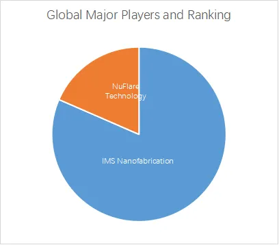
The multi-beam mask-writer market is the one segment with real reported revenue and paying demand. Third-party market research places 2022 to 2024 market value in the range of roughly USD 630 million to USD 960 million, with most estimates clustering near USD 800 million to USD 960 million and projected compound annual growth of roughly 7 to 12 percent through the early 2030s; QY Research estimated the 2024 market at USD 960 million growing to USD 2,084 million by 2031 at an 11.9 percent CAGR [3][45]. These are analyst figures rather than audited segment revenue, and should be treated as directional. The concentration: IMS is reported at 81.52 percent revenue share in 2024, with NuFlare the principal remaining supplier and JEOL a smaller player [3]. The demand driver is real and structural: EUV mask making and curvilinear ILT require the shape-independent write times only multi-beam writers provide, and leading fabs (TSMC, Samsung, Intel) run in-house mask shops that must equip with these tools [10].

5.2 Direct-write niches: paying demand versus aspiration
For direct wafer writing, the economics turn on the crossover volume below which eliminating the mask wins. A modern mask set at a leading node costs on the order of millions of dollars and takes weeks to fabricate; for low-volume or high-mix production, or for rapid design iteration, amortizing that cost over few wafers is prohibitive, and maskless direct write becomes attractive despite its low throughput [16]. This is the commercial logic for Multibeam and for e-beam direct write generally. The niches with the clearest paying or near-paying demand are: advanced-packaging redistribution layers and interposers (where Multibeam emphasizes sub-1-micron interconnects, large fields, and large depth of focus over topography) [12]; secure chip ID and device personalization (each die written uniquely, impossible with a fixed mask, valued for anti-counterfeit and supply-chain security, and aligned with defense Trusted-Supplier demand at SkyWater) [14][17]; photonics and quantum-device prototyping (curvilinear waveguides and qubit structures, small volumes, frequent redesign); and rapid prototyping and multi-project wafers [16]. The niches that remain more aspirational are any suggestion of mainstream logic or memory HVM direct write, which the throughput arithmetic rules out.
Mask writing has demonstrated invoiced demand at scale. Direct-write niches have early adoption (the SkyWater shipment, the historical Mapper-Leti security work) but the paying market is thin. ASML's Wennink assessed the maskless-unique-IC market at "one tool a year at most" [36], a view worth weighing against vendor optimism, though advanced packaging and secure provisioning may prove larger than that 2019 assessment implied.
6. Regulatory Landscape
The regulatory dimension is narrow, and centers almost entirely on export controls. Electron-beam mask writers and lithography tools fall under Category 3B of the US Commerce Control List, principally ECCN 3B001 (semiconductor manufacturing equipment) and related mask, reticle, and mask-substrate-blank provisions (3B001.g, .h, .j, .q), with associated software and technology in 3D001, 3D003, 3E001 and related ECCNs; computational-lithography and EUV-mask software and technology are specifically captured [46][47]. These derive substantially from Wassenaar Arrangement categories, transposed into the US EAR, Japanese METI controls, and Dutch national controls [48]. The October 2022 and October 2023 US rules, plus the September 2024 plurilateral framework, tightened controls on advanced-node equipment destined for China, including a "0 percent de minimis" rule for certain lithography equipment used in advanced-node IC production [46][47]. Beyond export control, there is no substantial sector-specific regulatory regime governing e-beam lithography tools; environmental, safety, and radiation-handling requirements are routine industrial matters and do not materially shape the competitive landscape.
7. Geopolitical and Strategic Dimensions
7.1 The IMS cap table and mask-writer access
The concentration of advanced mask writing in IMS (Intel-controlled, with TSMC and Bain minority stakes) and NuFlare (Japan) means that the single most critical enabling tool for EUV and curvilinear-ILT masks sits under US and Japanese control [29][11]. This is a bottleneck at least as strategically significant as the scanners themselves: without advanced mask writers, EUV scanners cannot be fed leading-edge masks. TSMC's minority stake in IMS, alongside Intel's majority, reflects the mutual dependence of rival leading-edge manufacturers on a shared, single-source tool, and gives both a seat at the table while leaving ultimate control with Intel [30]. For an acquirer or policymaker, IMS is arguably a more concentrated point of leverage than any single equipment category except EUV light sources and optics.
7.2 Japan's position
Japan holds a strong hand through NuFlare (mask writers and the VSB installed base) and Advantest (test, and historical e-beam), plus JEOL [3][11]. Japanese METI export controls are coordinated with US measures [48]. NuFlare's position as the principal alternative to IMS gives Japan durable leverage in the mask-writing bottleneck.
7.3 China indigenization and the "e-beam as EUV workaround" narrative
In August 2025 the Hangzhou municipal government announced "Xizhi," described as China's first commercial electron-beam lithography machine, developed by Zhejiang University's Yuhang Quantum Research Institute [49]. It is a 100 kV system claimed to achieve 0.6nm positioning accuracy and 8nm line width, aimed explicitly at quantum-chip and next-generation semiconductor R&D, and marketed as filling a gap created by export controls that had denied Chinese institutions (the University of Science and Technology of China, Zhejiang Lab) access to imported e-beam tools [49][50].
The "workaround to EUV denial" framing does not survive quantitative scrutiny, and CSIS assessed the announcement as revealing "more exaggeration than transformation in terms of leading competitive capabilities" while still showing "gradual progress" [4]. Xizhi, like all e-beam direct-write tools, is a serial (or modestly parallel) maskless writer whose throughput is orders of magnitude below EUV. It is useful for research, prototyping, mask making, and quantum-device fabrication, but CSIS judged it "ill-suited for the high-volume chip production required to power advanced AI systems" [4]. The arithmetic from Section 4.4 is decisive: even the most ambitious massively parallel maskless designs (Mapper's never-achieved 10 wafers per hour) fall 250-plus times short of a single EUV scanner's output per tool, and Xizhi is a single-column-class R&D tool far below even that. For military or commercial classes of chips where volumes are very low and designs unique (radiation-hardened ASICs, certain secure or specialized devices, quantum prototypes), a maskless e-beam route is a legitimate capability, and that is precisely the niche Xizhi targets. For the leading-edge logic and memory that drive AI compute, it is not a substitute for EUV. China's e-beam effort is a sensible move to secure a research-and-prototyping and secure-provisioning capability under sanctions, not a breakthrough that neutralizes the EUV bottleneck.
8. Risk Matrix
| Risk | Category | Likelihood | Impact | Mitigation |
|---|---|---|---|---|
| Direct-write throughput never improves enough to expand beyond niche | Technical | High | High for direct-write vendors; low for mask-writer segment | Focus on niches where maskless economics already win (packaging, secure ID, prototyping); do not underwrite HVM logic use cases |
| Multibeam tool performance underperforms vendor throughput claims in the field | Technical/Commercial | Medium | High for Multibeam and early adopters | Insist on independently verified throughput at specified node and dose before qualification; stage purchases |
| Single-source dependence on IMS for advanced mask writers | Supply chain | Medium | Very high (feeds all EUV mask making) | Qualify NuFlare as second source; maintain VSB fallback for less advanced nodes |
| Export-control tightening removes China from addressable market for leading-edge tools | Geopolitical | High (already occurring) | Medium (China is a minority of leading-edge mask-writer demand) | Vendors diversify to allied-market demand; price in reduced China TAM |
| Chinese indigenization erodes mid-tier and legacy e-beam and mask-writer demand over 5-10 years | Geopolitical/Commercial | Medium | Medium | Incumbents defend on leading-edge performance where China lags most |
| Data-path and stitching engineering barriers stall multi-column scale-up | Technical | Medium | Medium | Continued investment in on-tool compression, decoder parallelism, and in-situ registration calibration |
| A further direct-write entrant collapses (repeat of Mapper/REBL), chilling investment | Commercial | Medium | Medium | Investors treat direct-write as venture-risk, not infrastructure; require niche revenue traction |
9. Strategic Recommendations
9.1 For institutional investors and corporate strategists
Distinguish the two markets sharply. The multi-beam mask-writer segment is a growing, highly concentrated infrastructure business with invoiced revenue and a structural EUV-driven tailwind; exposure to it: (principally through IMS's ownership by Intel and stakes held by TSMC and Bain, and through NuFlare via Toshiba). Treat direct-write multi-column ventures (Multibeam) as venture-stage bets on specific niches, not as plays on displacing optical or EUV HVM; the base rate of failure (Mapper, REBL, SCALPEL, PREVAIL) is high. The benchmark that would change this posture is independently verified direct-write throughput and yield at a named node and dose sufficient to demonstrate positive unit economics in a paying niche such as advanced-packaging RDL or secure provisioning. Absent that, size positions to survive a Mapper-style outcome. Monitor the IMS cap table: any move by Intel to divest control, or by a single foundry to increase its stake, would be strategically important.
Staged triggers: (1) if Multibeam or a peer publishes third-party-verified throughput above roughly 10 wafers per hour at a specified advanced node with acceptable placement error, re-rate the direct-write opportunity upward; (2) if IMS ownership consolidates or fragments, reassess bottleneck exposure; (3) if China's domestic mask-writer capability reaches the 5nm-node class, discount incumbents' mid-tier China revenue.
9.2 For foundry, mask-shop, and advanced-packaging technologists
For mask shops at advanced and EUV nodes, multi-beam mask writers are no longer optional; qualify IMS as the primary and NuFlare as a second source to mitigate single-source risk, and retain VSB capacity for nodes where its economics still hold. The decision threshold is pattern complexity and node: once curvilinear ILT or sub-7nm CDU requirements dominate, multi-beam is mandatory because write time becomes complexity-independent.
For advanced-packaging and specialty technologists, evaluate multi-column direct write (Multibeam) specifically where mask elimination wins: sub-1-micron RDL and interposers at low-to-medium volume, chiplet-unique or die-unique patterning, secure chip ID, photonics, and quick-turn prototyping. Qualify against measured throughput and placement accuracy on your actual layers, not vendor headline figures, and pilot on a single high-value use case (secure provisioning or a photonics prototype line) before committing to production integration. The threshold that justifies scale-up is demonstrated cost per wafer pass below the amortized mask-plus-cycle-time cost of the optical alternative at your specific volume and redesign cadence.
9.3 For policymakers concerned with export-control design
Recognize that the advanced mask writer, not only the scanner, is a bottleneck, and that it is currently concentrated in IMS and NuFlare. Controls that focus solely on scanners while neglecting mask writers and their data-preparation software would leave a gap. At the same time, calibrate expectations about e-beam direct write: the "EUV workaround" narrative around tools like Xizhi is not quantitatively credible for HVM, so control regimes should weight e-beam direct-write tools as R&D, prototyping, and secure-provisioning capabilities (still strategically relevant, especially for defense-relevant low-volume chips) rather than as HVM substitutes. The Mapper episode, in which the Pentagon reportedly pushed to keep assets from Chinese buyers, is a template: asset-level vigilance during bankruptcies of unique-capability firms is a low-cost, high-value intervention.
10. Caveats
Several figures in this report are vendor assertions or analyst projections rather than measured, independently verified data, and are labeled as such. Multibeam's throughput range (2 to 25 wafers per hour per module) and its comparative claims are vendor figures; no peer-reviewed independent tool-performance data were identified. Market-size figures for multi-beam mask writers come from commercial syndicated-research firms whose methodologies are not fully transparent and which disagree by up to roughly 50 percent; they are directional. The Xizhi specifications are from Chinese government and media sources and have not been independently verified. Some throughput derivations in Section 4.4 (units needed to match an EUV scanner, annual wafer output) are the author's arithmetic built on sourced per-tool figures, not quotations from a single analyst study. The Mapper acquisition price (about EUR 75 million) and the Pentagon-intervention account derive from press reconstruction and should be treated as reported rather than confirmed. Finally, the direct-write niche market's true size is uncertain: it sits between a credible floor (demonstrated early shipments) and vendor optimism, and the evidence base is too thin to size it precisely.
Further Reading:
 John D

 John D
 Contributors to Wikimedia projects
 John D
 John D
References
- Pain, L., S. Tortai, S. Minghetti, et al. 2006. "Transitioning of Direct e-Beam Write Technology from R&D into Production Flow." Microelectronic Engineering. (Reports ~50-60 hours per 300mm wafer at the 65nm node for a variable-shaped-beam column.)
- ASML Holding N.V. 2025. Form 6-K Annual Report (FY2025), U.S. Securities and Exchange Commission. ("TWINSCAN NXE:3800E systems... 220 wafers-per-hour throughput – a 37% improvement compared to the TWINSCAN NXE:3600D.")
- QY Research. 2025. "Multi-beam Mask Writer – Global Market Share and Ranking, Overall Sales and Demand Forecast 2025-2031." (IMS revenue share 81.52% in 2024; market USD 960 million in 2024; Advantest niche positioning per corroborating market-research sources.)
- Wentz, Jacob, and Anita Lin. 2025. "Breakthroughs or Boasts? Assessing Recent Chinese Lithography Advancements." Center for Strategic and International Studies (CSIS), Strategic Technologies Blog, September 24.
- Science.gov topic compilation (drawing on IMS Nanofabrication publications). "Electron Beam Lithography." (History of IBM shaped-beam direct write, Coulomb-interaction limits, EPL programs, and 2003 Nikon PREVAIL stepper shipment to Selete.)
- U.S. Patent 6,069,684, "Electron Beam Projection Lithography System (EBPS)." (Coulomb-interaction blur scaling with current and voltage; shot-noise dose limit discussion.)
- U.S. Patents 6,870,172 and 7,692,167. (State that writing an entire wafer by electron-beam direct write may take ten to one hundred hours.)
- Wieland, M. J., et al. 2008. "MAPPER: High Throughput Maskless Lithography." Proceedings of SPIE Vol. 6921. (Shot-noise dose figure: ~4,000 electrons per 45nm pixel, ~30 microcoulombs per square centimeter.)
- Yasuda, Hiroshi, Takeshi Haraguchi, and Akio Yamada (Advantest). 2004. "A Proposal for an MCC (Multi-Column Cell with Lotus Root Lens) System to Be Used as a Mask-Making e-Beam Tool." Proceedings of SPIE Vol. 5567, 24th BACUS Symposium.
- Tomandl, Mathias, Christoph Spengler, Peter Hudek, Christof Klein, Hans Loeschner, and Elmar Platzgummer (IMS Nanofabrication). 2024. "Multi-beam Mask Writing Opens Up New Fields of Application, Including Curvilinear Mask Pattern for High Numerical Aperture Extreme Ultraviolet Lithography." Journal of Micro/Nanopatterning, Materials, and Metrology 23 (1): 011205.
- Matsumoto, Hiroshi, Hideo Inoue, Hiroshi Yamashita, et al. (NuFlare Technology). 2016. "Multi-beam Mask Writer MBM-1000 and Its Application Field." Proceedings of SPIE Vol. 9984, Photomask Japan 2016, 998405. (Includes MBM-2000PLUS specifications from subsequent NuFlare BACUS publications.)
- Multibeam Corporation. "Applications." Accessed 2026. multibeamcorp.com/applications. (Advanced-packaging interposers, large depth of focus, on-wafer die-die stitching.)
- Science.gov topic compilation. "Electron-Beam Projection Lithography." (Field curvature and Coulomb interaction as fundamental limits of SCALPEL and PREVAIL.)
- Multibeam Corporation. Wikipedia and multibeamcorp.com/about. Accessed 2026. (Founding by David K. Lam in 2010; all-electrostatic miniature columns; CEBL, Secure Chip ID, advanced packaging, photonics targets.)
- Lapedus, Mark. "Multibeam Obtains Funding for Next-Gen E-Beam Lithography." marklapedus.substack.com. (5 kV beam energy; 2-25 wafers per hour per module; >100 micron depth of focus; investors Onto Innovation, Lam Capital, UMC Capital, MediaTek Capital.)
- Synopsys. "Powering Electron Beam Lithography with Multibeam" and "Multibeam: Innovation with E-Beam Lithography." Accessed 2026. (Maskless direct write, faster yield ramp, no mask wait; data-prep integration.)
- SkyWater Technology. 2024. "SkyWater Announces Enhanced Capabilities with Multibeam's First-in-Industry High-Productivity Multicolumn E-Beam Lithography System." Business Wire, July 25.
- Multibeam Corporation. 2024. Stevie Awards entry, "Groundbreaking Semiconductor Manufacturing Technology." (46 awarded US patents.)
- Takahashi, Dean. 2024. "Multibeam Launches Chip Industry's 1st Multicolumn E-Beam Lithography." VentureBeat. (Lam "100 times more productive" statement.)
- Komami, T., et al. (Advantest). 2011. "MCC8: Throughput Enhancement of EB Direct Writer." Microelectronic Engineering / SPIE Advanced Lithography. (8 column cells, 5 wafers per hour; 6-unit cluster >30 wafers per hour; four-column MCCPOC built March 2010 under ASET/NEDO.)
- Yamada, A., et al. (Advantest). "Study of Device Mass Production Capability of the Character Projection Based Electron Beam Direct Writing Process Technology toward 14nm Node and Beyond." (100 wafers per hour target: 150 beams, 10 clusters, 100 giga-shots per wafer, 250 A/cm2, 75 microcoulombs per square centimeter.)
- Association of Super-Advanced Electronics Technologies (ASET), Mask-D2I program publications. (MCC proof-of-concept mix-and-match overlay better than 5nm; NEDO sponsorship.)
- Chang, T. H. P., et al. 1996. "Electron Beam Technology—SEM to Microcolumn." Microelectronic Engineering 32: 113-130. (Microcolumns ~3.5mm long, 10nm probe at ~1 nA and 1 keV.)
- Chang, T. H. P., et al. 1992. "Arrayed Miniature Electron Beam Columns for High Throughput Sub-100 nm Lithography." Journal of Vacuum Science & Technology B 10 (6): 2743-2748.
- Muray, L. P., K. Y. Lee, J. P. Spallas, et al. 2000. "Experimental Evaluation of Arrayed Microcolumn Lithography." Microelectronic Engineering; and Kratschmer, E., et al. 1996. "Experimental Evaluation of a 20×20 mm Footprint Microcolumn." Journal of Vacuum Science & Technology B 14 (6): 3792-3796.
- Klein, Christof, Elmar Platzgummer, et al. (IMS Nanofabrication). 2016. "MBMW-101: World's 1st High-Throughput Multi-Beam Mask Writer." BACUS/SPIE Photomask Technology. (262,000 beams, 20nm beam size, 1 A/cm2, up to 1 microamp, 120 Gbit/s data path, full-field 7nm layouts in under 10 hours.)
- IMS Nanofabrication GmbH. "Products" and MBMW-301 SPIE materials. Accessed 2026. ims.co.at. (Generational timeline MBMW-101/201/301; MBMW-100 Flex node range.)
- Tekscend Photomask Germany GmbH and IMS Nanofabrication. 2024. "Tekscend Photomask and IMS Nanofabrication Unveil Europe's First Multibeam Mask Writer at AMTC Dresden." Press release, November 12. (MBMW-100 Flex reduces mask write time to 7-12 hours.)
- Intel Corporation. 2023. "Intel to Sell Minority Stake in IMS Nanofabrication Business to TSMC." Press release / Intel Newsroom, September 12. (10% to TSMC at ~USD 4.3 billion valuation; prior 20% to Bain Capital; Intel initial investment 2009, full acquisition 2015; CEO Elmar Platzgummer.)
- VentureBeat and Intel FY2023 filings. 2023. "Intel Sells Stake in IMS Nanofabrication to TSMC for $430M." (USD 430 million for 10%; USD 860 million for 20% to Bain; combined ~USD 1.4 billion net proceeds for 32%.)
- Wieland, M. J., et al. 2013. "MAPPER: Progress toward a High-Volume Manufacturing System." Proceedings of SPIE Vol. 8680. (13,260 parallel beams delivering 170 microamps; each beam 49 sub-beams; >10 wafers per hour target at 22nm.)
- Wieland, M. J., et al. 2010. "Throughput Enhancement Technique for MAPPER." Proceedings of SPIE Vol. 7637. (Dispenser cathode ~0.3 nA per beam at 25nm spot; factor ~50 below 13 nA required for 10 wafers per hour.)
- Lapedus, Mark. 2019. "Manufacturing Bits: Feb. 5" and related. Semiconductor Engineering. (Mapper FLX-1200, MEMS blanker; ASML acquisition; KLA exit around 2014; Mapper Moscow MEMS fab.)
- ASML Holding N.V. 2019. "ASML Agrees to Acquire Mapper Assets and Intends to Offer Continued Employment to Staff." GlobeNewswire, January 28. (Mapper declared bankrupt December 28, 2018; IP acquisition; staff into R&D and product assembly.)
- Reuters (via Cyprus Mail), December 10, 2024, citing Focus: The ASML Way (2024). ("ASML bought Mapper... for 75 million euros ($79 million) in 2019.")
- Bits&Chips. 2019. "Pentagon Pushed for ASML's Acquisition of Mapper." (Pentagon urged Dutch intervention; Mapper's China outreach; Wennink "one tool a year at most"; ASML's ~2000 conclusion on e-beam throughput.)
- Petric, Paul, Chris Bevis, Mark McCord, et al. (KLA-Tencor). 2009. "Reflective Electron Beam Lithography (REBL): A Novel Approach to High Speed Maskless Ebeam Direct Write Lithography." Journal of Vacuum Science & Technology B 27 (1): 161; and Petric et al. 2010, JVST B 28 (6): C6C6-C6C13. (5-7 wafers per hour at 45nm; DPG >1 million pixels; DARPA Maskless Nanowriter program.)
- "New Advances with REBL for Maskless High-Throughput EBDW Lithography." Proceedings of SPIE Vol. 7970. (Wien-filter column; 36-column configuration; ~1 Tbit/s data rate.)
- ASML. "HMI eScan 1000" and "HMI eScan 1100 – Metrology & Inspection Systems." Accessed 2026. asml.com. (9-beam 3x3 array; 25-beam, up to 15x faster than single-beam inspection.)
- ASM International. 2016. "ASML to Acquire HMI for Semiconductor Inspection and E-beam Metrology." (~USD 3 billion cash transaction.)
- Carl Zeiss SMT. "ZEISS MultiSEM – Multi-Beam Electron Microscope." Accessed 2026. zeiss.com; and Kemen, T., et al. 2015. "Further Advancing the Throughput of a Multi-Beam SEM." (91 parallel beams; >3 terabytes per hour; pixel rates over 1.5 GHz.)
- Platzgummer, Elmar, Christof Klein, and Hans Loeschner. 2013. "Electron Multibeam Technology for Mask and Wafer Writing at 0.1 nm Address Grid." Journal of Micro/Nanolithography, MEMS, and MOEMS 12 (3): 031108. (>2 milliamps to wafer for 100 wafers per hour; 50-100 sub-columns and 10-20 clustered tools.)
- Savari, Serap A., et al. 2016. "Impact of Parallelism on Data Volumes for a Multibeam Mask Writer." Journal of Vacuum Science & Technology B 34 (6): 06KF01. (512×511 beam array ~261,000 beams; ~1 terabit per second at 1 MHz deflection; petabyte data volumes.)
- Klein, Christof, et al. (IMS Nanofabrication). "Performance of the Proof-of-Concept Multi-Beam Mask Writer." (Registration within 82×82 micron beam-array field; ~1.3nm 3-sigma short-term repeatability, LMS IPRO4.)
- Multiple market-research publishers (Data Insights Market, Intel Market Research, Verified Market Reports, Dataintelo). 2024-2025. Multi-beam mask writer market sizing reports. (Range USD 630 million to USD 960 million for 2022-2024; CAGR ~7-12%.)
- K&L Gates. 2023. "US Government Revises Comprehensive Export Controls on Semiconductors and Semiconductor Manufacturing Equipment." (ECCN 3B001.f; 0% de minimis rule for advanced-node lithography equipment.)
- Covington & Burling LLP. 2024. "U.S. Implements Plurilateral Export Controls Framework and Additional Controls on Semiconductor, Quantum, and Additive Manufacturing Items." (ECCNs 3B001.g/.h/.j/.q, 3D001, 3E001; EUV mask and reticle software/technology.)
- U.S. Bureau of Industry and Security / Federal Register. 2020, 2023. "Implementation of Certain New Controls on Emerging Technologies Agreed at Wassenaar Arrangement 2019 Plenary" and "Export Controls on Semiconductor Manufacturing Items." (Wassenaar basis of lithography-tool and mask-substrate controls.)
- Hangzhou Municipal Government. 2025. "China Unveils First Homegrown Electron Beam Lithography Machine." ehangzhou.gov.cn, August 15; corroborated by TrendForce and Global Times. (Xizhi, 100 kV, 0.6nm accuracy, 8nm line width, Zhejiang University Yuhang Quantum Research Institute.)
- South China Morning Post. 2025. "China Debuts First E-beam Lithography Machine for Commercial Use in Chipmaking Milestone." (Export-control context; institutions previously denied access.)