The Semiconductor Lithography Landscape 2026: A Complete Taxonomy of Patterning Technologies Organized by Commercialization Maturity
A maturity-ranked taxonomy of chip patterning, from dead NGL contenders to High-NA EUV, and why value concentrates in ASML's monopoly stack.

As of September 25, 2026.
1. Summary
Value in the patterning stack through 2030 concentrates overwhelmingly in a small number of monopoly and near-monopoly positions anchored by extreme ultraviolet (EUV) lithography, and investors should treat ASML (NASDAQ: ASML) and its ecosystem of single-source suppliers as the structural core of the thesis, with disruption confined to specific, bounded niches rather than a wholesale displacement of the incumbent stack [1][2][45]. ASML is the sole manufacturer of EUV exposure tools, recognized revenue on 48 EUV systems in 2025, and closed the year with total net sales of €32.7 billion and a backlog of €38.8 billion [1][3]. The company's High-NA 0.55 numerical aperture platform is now in production use: Intel runs High-NA on select critical layers of its 18A Panther Lake processors and has processed more than one million wafers on the platform, and as of September 2026 ten High-NA systems were operating at four customers with three more in shipment or installation [45][47][48]. The adoption question has shifted from whether to when. TSMC, which kept High-NA off every node on its roadmap through 2029 on cost grounds, committed in September 2026 to High-NA in high-volume manufacturing from 2030, while Samsung and SK Hynix are targeting DRAM production use around 2028 [46][55][56].
The second finding is that the durable monopoly rents lie not only in the scanner but in the surrounding single-source layers: EUV mask blanks (an AGC and Hoya duopoly holding approximately 93 percent of the market, with AGC alone above 59 percent), EUV light sources (ASML's captive Cymer unit), computational lithography (concentrated in ASML Brion, Synopsys, Siemens EDA and Cadence), metrology and inspection (KLA at over 56 percent of the global process-control, metrology and inspection segment and above 85 percent of optical wafer inspection), resist chemistry (a Japanese-led oligopoly of JSR, Tokyo Ohka Kogyo, Shin-Etsu, Fujifilm and Sumitomo), and photoresist tracks (Tokyo Electron at 92 percent of coater/developer systems and 100 percent of the EUV segment) [6][7][8][9]. These are the least contested positions in the entire stack.
The third finding is that credible disruption is narrow: nanoimprint lithography (Canon's FPA-1200NZ2C) is a cost and power alternative confined for now to memory and evaluation use; multi-beam mask writers (IMS Nanofabrication, owned by Intel, and NuFlare, part of Toshiba) have already displaced variable-shaped-beam tools for the most advanced EUV mask writing; multi-column direct-write e-beam (Multibeam Corporation) addresses high-mix low-volume and advanced-packaging niches; and directed self-assembly (DSA) is re-emerging specifically as an EUV rectification and pitch-multiplication complement, not a standalone replacement [10][11][12][13]. The fourth finding is that the entire structure is now shaped by export controls and Chinese indigenization: EUV has never been officially exported to China, DUV immersion is license-controlled, and China's steady-state micro-bunching and laser-induced-discharge-plasma EUV efforts remain at laboratory or prototype stage with a commercial gap measured in years [14][15]. The lesson from the failed next-generation lithography (NGL) races (proximity X-ray, SCALPEL, electron and ion projection) is transferable and directly relevant to every current contender: source power economics, throughput, ecosystem readiness and defectivity decide these races, not resolution physics alone [16][17].
On July 15th, 2026, ASML raised full-year 2026 guidance to €43 billion to €45 billion and plans to ship around 65 low-NA EUV systems in 2026. Q2 net sales were €9.3 billion at a 54.0% gross margin. ASML plans to add 30% to its roughly 65-unit low-NA EUV capacity for 2027 and is investigating another 30% for 2028. It plans the same 30% increase for its roughly 130-unit DUV immersion capacity.
2. Background: The Physics and Economics That Make the Taxonomy Legible
The organizing equation for optical lithography is the Rayleigh criterion, in which the minimum resolvable half-pitch equals k1 multiplied by the wavelength and divided by the numerical aperture. Resolution therefore improves by shrinking the wavelength, raising the numerical aperture, or reducing the process factor k1, which has a hard single-exposure physical floor near 0.25 and is pushed lower in practice only by multiple patterning. This single relationship explains the entire history of the field: the progression from i-line (365 nm) through KrF (248 nm) and ArF (193 nm), the leap to ArF immersion (a 1.35 effective numerical aperture achieved by placing water between the final lens and the wafer), the resort to double, triple and quadruple patterning when 193i ran out of single-exposure resolution, and finally the discontinuous jump to EUV at 13.5 nm. High-NA EUV raises the numerical aperture from 0.33 to 0.55, and the proposed Hyper-NA extension contemplates 0.75 or higher [4][18].
The economics that decide adoption are throughput (wafers per hour), source power (which sets throughput for EUV), and cost per wafer pass. A single EUV exposure that replaces three or four DUV patterning passes can lower net cost and defect risk even at a far higher tool price, which is the entire commercial logic of EUV; conversely, when a High-NA exposure costs materially more than the multi-patterned DUV or standard-EUV alternative it displaces, adoption stalls until the density benefit justifies the premium. Depth of focus, which shrinks with the square of the numerical aperture, and stochastic (photon-shot-noise) defects, which worsen as features shrink and doses stay finite, are the two physical penalties that dominate the leading edge and drive the resist and computational-lithography markets.
3. Key Players
The exposure-tool layer is effectively a monopoly at the leading edge. ASML is the sole EUV supplier and dominates ArF immersion, holding roughly 90 percent of the immersion market by ASML's own account, and around 80 to 90 percent of the total lithography market by revenue [19][20]. Nikon and Canon (TYO: 7733; TYO: 7751) share the remainder: Nikon retains a minority ArF immersion presence and has announced a new immersion platform for its fiscal 2028 designed for compatibility with ASML masks, while Canon leads i-line at roughly 80 percent share, is the number-two lithography vendor by unit volume (233 systems in 2024), and is the sole commercial supplier of semiconductor nanoimprint tools [20][21][10].
In the surrounding layers, the light source for EUV is ASML's captive Cymer unit, with Gigaphoton and Ushio (TYO: 6925) supplying DUV excimer sources. EUV mask blanks are an AGC (TYO: 5201) and Hoya (TYO: 7741) duopoly [6][22].
Pellicles and mask infrastructure draw in Mitsui Chemicals (TYO: 4183) and Canatu in partnership with imec [7]. Resist chemistry is led by JSR privately held, parent of metal-oxide specialist Inpria), Tokyo Ohka Kogyo (TYO: 4186), Shin-Etsu Chemical (TYO: 4063), Sumitomo Chemical (TYO: 4005) and Fujifilm (TYO: 4901), with Lam Research (NASDAQ: LRCX) pushing dry resist via its Aether platform [8][23]. Track (coater/developer) systems are dominated by Tokyo Electron (TYO: 8035) at 92 percent, with SCREEN Holdings (TYO: 7735) second [9].
Metrology and inspection: led by KLA (NASDAQ: KLAC), with Onto Innovation (NYSE: ONTO), Bruker (NASDAQ: BRKR), Applied Materials (NASDAQ: AMAT) and Carl Zeiss SMT (private, the sole EUV optics supplier to ASML) as material participants [24][7]. Computational lithography concentrates in ASML Brion, Synopsys (NASDAQ: SNPS), Siemens EDA and Cadence (NASDAQ: CDNS) [25]. Mask writers are supplied by IMS Nanofabrication (owned by Intel, NASDAQ: INTC) and NuFlare (part of Toshiba). Direct-write is pursued by Multibeam Corporation (private). Chinese domestic efforts center on SMEE, its packaging spin-off AMIES, SiCarrier and Yuliangsheng, with Huawei-linked and academic (Tsinghua, Harbin Institute of Technology) source research [15][14].
4. Technical and Operational Considerations: The Taxonomy by Commercialization Maturity
4.1 The Dead Contenders and Their Transferable Lesson
Four next-generation lithography programs that once looked like credible successors to optical lithography are now dead, and they earn coverage only because their failure modes recur in today's contenders. Proximity X-ray lithography, favored in 1990s cost-of-ownership models precisely because it looked cheapest when several steppers shared a synchrotron storage ring, died from the impracticality of 1:1 masks and the infrastructure burden [16]. SCALPEL (scattering with angular limitation projection electron-beam lithography), developed at Lucent's Bell Labs, and the parallel PREVAIL electron projection program pursued by IBM and Nikon, both foundered on the fundamental throughput ceiling of electron projection: space-charge effects and limited beam current meant they could never match optical throughput, exactly as contemporary cost-of-ownership models warned [17][16]. Ion projection lithography (IPL) failed on the need for complementary masks and beam-current limits [16]. The transferable lesson is precise and it is the analytic spine of this report:
NGL races are decided by source power economics, throughput, ecosystem readiness (masks, resists, metrology) and defectivity, and a technology can hold a resolution advantage yet still lose decisively on those four axes.
EUV itself nearly failed on source power, spending roughly two decades between the 1997 EUV LLC consortium and TSMC's 2020 production insertion, and only survived because ASML sustained the source-power roadmap from single-digit watts to the several-hundred-watt regime [26][15].
4.2 The Incumbent Optical Family: Defending a Vast, Profitable Niche
The i-line (365 nm) and KrF (248 nm) families are mature, not obsolete: they pattern analog, power, MEMS, image sensors and the non-critical layers of advanced chips, and they persist because they are cheap, high-throughput and fully depreciated. Canon holds roughly 80 percent of i-line [20]. ArF dry (193 nm) serves mid-critical layers. ArF immersion (193i), with an effective numerical aperture of 1.35 and a single-exposure resolution near 38 nm half-pitch, remains the workhorse of the industry: the majority of patterning steps even on a 3 nm chip still run on 193i, extended to roughly 7 nm-class logic through self-aligned double and quadruple patterning (SADP, SAQP) [20][15]. The strategic trajectory of the optical family is a durable, defended niche: expanding in absolute unit terms with fab construction and advanced packaging, but structurally displaced from the leading edge by EUV. ASML dominates 193i (about 90 percent), and Nikon's fiscal-2028 re-entry attempt targets exactly this segment on price [19][21].
 John D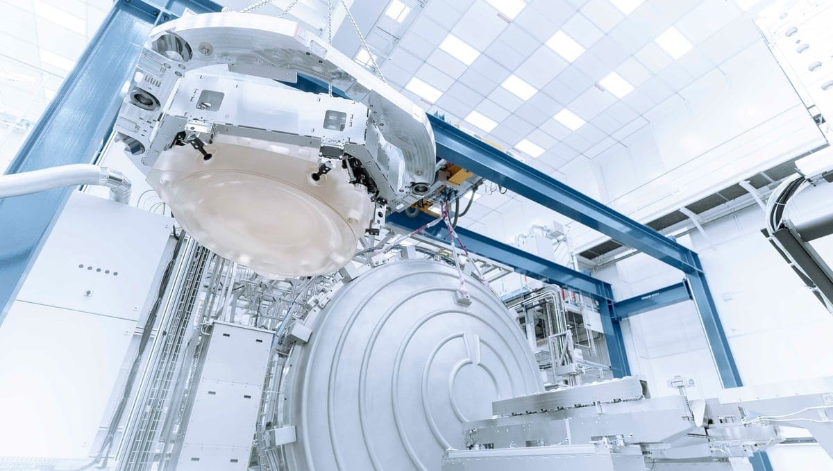
4.3 The EUV Family: The Monopoly Core
Standard 0.33 NA EUV (13.5 nm wavelength) resolves roughly 13 nm half-pitch in single exposure and is the incumbent leading-edge tool. ASML's current-generation NXE:3800E processes over 195 wafers per hour at 30 mJ/cm2 dose, rising to 220 with upgrades, with matched-machine overlay below 1.1 nm, at a unit price near 180 million dollars [27][28]. Source power is the binding throughput constraint; ASML has demonstrated a 1,000-watt source in the laboratory and projects a path to 330 wafers per hour by 2030, which are developer projections rather than shipped performance [29]. This platform is the single most profitable position in the industry and faces no credible competitor before 2030.
High-NA 0.55 NA EUV (the EXE platform) resolves about 8 nm half-pitch and enables transistor density up to 2.9 times higher than 0.33 NA, letting chipmakers collapse what would be three EUV exposures into one [4][18]. The EXE:5200B production tool delivers about 175 wafers per hour, a 60 percent productivity gain over the EXE:5000, with overlay near 0.7 nm, priced near 380 million dollars, roughly double a standard EUV tool [5][28]. The installed base remains small but is now in production. Five EXE:5000 R&D units preceded the first EXE:5200B, shipped in early 2025; by September 2026 ASML reported ten High-NA systems operating at four customers, with three more in shipment or installation, and a target of 90 percent fleet availability by the fourth quarter of 2026 [30][48]. Intel completed EXE:5200B acceptance in late 2025, began high-volume shipment of Panther Lake products with High-NA on select 18A layers in July 2026, and reported more than one million cumulative High-NA wafers in September 2026, a figure that includes tool qualification and development as well as production [45][47].
TSMC declined High-NA for A14 and for its 2029 A12 and A13 nodes, extending 0.33 NA EUV with multi-patterning, but in September 2026 committed to High-NA in high-volume manufacturing from 2030. It is also co-leading an industry initiative with ASML to move from 6-inch to 12-inch photomasks, targeting a pilot line by 2031 and production readiness by 2033 [46][56]. The larger mask addresses a real throughput penalty: at today's 6-inch mask size, High-NA's half field forces large dies to be stitched from two exposures, which Intel data presented at SPIE indicate cuts throughput from roughly 175 to roughly 125 wafers per hour [57]. The strategic trajectory is expanding, with a customer-staged timeline that is now committed rather than contested: memory around 2028, and the largest foundry from 2030. The demonstrated resolution is proven; the insertion timeline is customer-specific and, for the largest foundry, deliberately deferred.

Hyper-NA, defined as above 0.75 NA, would enable scaling past the A7 node, which is expected to reach HVM around 2033, with the NA increase needed around the second half of the 2030s. ASML has explicitly framed it as a vision with feasibility studies ongoing rather than a committed product [31][18]. The physics obstacles are concrete: depth of focus shrinks with the square of the numerical aperture, and above 0.55 NA light polarization begins to cancel imaging contrast, requiring polarizers that block light and reduce power efficiency [31][18]. imec targets an 18 nm metal pitch for High-NA and notes Hyper-NA could reach pitches well below 20 nm [18]. Hyper-NA should be treated as an aspirational roadmap item, not a demonstrated capability.
4.4 The Electron-Beam Family: Indispensable in Mask Making, Niche on Wafers
Electron-beam lithography spans Gaussian-beam and variable-shaped-beam (VSB) direct-write, cell projection, and the newer multi-beam and multi-column architectures. Its resolution is set by the beam diameter and electron scattering rather than a wavelength, so it reaches sub-10 nm, but its throughput ceiling (the same space-charge and current limit that killed SCALPEL and PREVAIL) confines wafer direct-write to research, prototyping and specialty production.
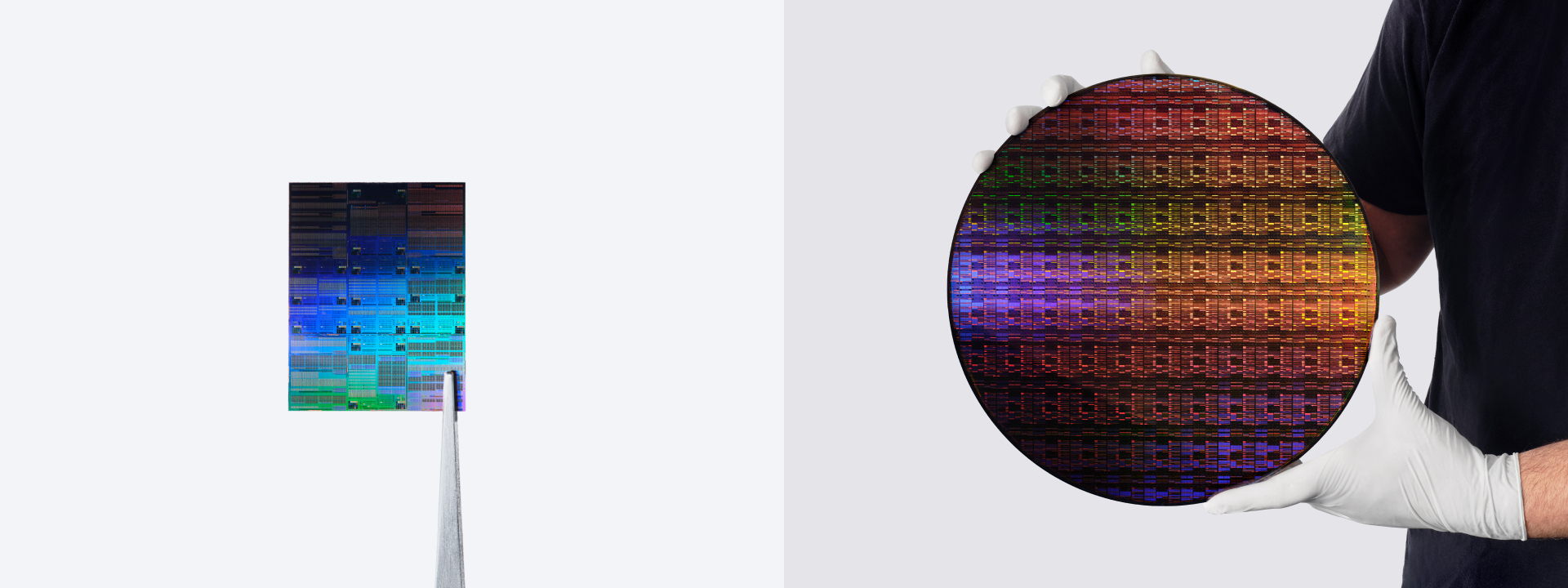
The commercially decisive development is multi-beam mask writing: IMS Nanofabrication shipped the first multi-beam mask writer and held 81.52 percent of that market in 2024, with NuFlare (Toshiba) the challenger [11][32]. Multi-beam writers use thousands of parallel beams to hold EUV mask write time below 10 hours regardless of pattern complexity, which is essential for curvilinear inverse-lithography-technology (ILT) masks that VSB tools cannot write economically; this cut mask write times from around 40 hours to below 10 [11][32]. Multibeam Corporation's multi-column direct-write (MEBL) platform, shipped to SkyWater (NASDAQ:SKYT), targets high-mix low-volume production, advanced-packaging interposers, photonics and secure chip ID, claiming a 10x to 100x productivity gain over conventional single-beam e-beam; ASML's acquisition of the bankrupt Mapper direct-write assets in 2019 folded that lineage into the incumbent [12][33]. The strategic trajectory is expanding in mask making (multi-beam displacing VSB) and holding a defended niche on wafers; direct-write is not a volume-logic threat to EUV.
 John D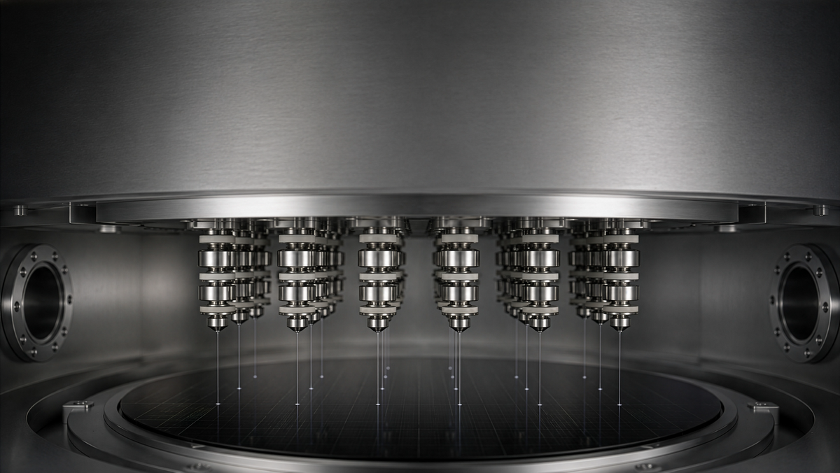
4.5 The Ion-Beam Family: A Precision Tool, Not a Patterning Platform
Focused ion beam (FIB) and helium/neon gas-field-ion-source approaches offer resolution limited by beam diameter rather than wavelength, reaching the sub-10 to 20 nm regime on test structures, but they are inherently serial and low-throughput [34][35]. Their commercial role is mask repair, circuit edit and nanofabrication research, not device patterning: gallium FIB is the established mask-repair tool, and helium/neon beams are studied for EUV mask editing, though they induce subsurface damage to the Mo/Si multilayer that constrains use [36][34]. The trajectory is a stable, indispensable niche adjacent to lithography rather than a patterning contender.
4.6 Nanoimprint Lithography: The Genuine but Bounded Cost Disruptor
Canon's Jet and Flash Imprint Lithography (J-FIL), commercialized as the FPA-1200NZ2C in October 2023 and first shipped commercially to the Texas Institute for Electronics in September 2024, patterns by pressing an inkjet-deposited UV-curable resist against a mask template, eliminating the wavelength constraint entirely [10][37]. It achieves a 14 nm minimum linewidth (5 nm-node-equivalent), and Canon's roadmap targets 10 nm and below via advanced template technology [10]. Canon claims roughly one-tenth the power consumption of EUV and a cost per system reportedly an order of magnitude below EUV [38]. Kioxia has tested NIL for several years and is evaluating it for prototype memory; SK hynix and Micron have expressed interest, reflecting NIL's suitability for the repetitive layers of memory over logic [10][37]. The material risks are defectivity (direct template contact prints defects), overlay, and template lifetime; Canon's roadmap targets specific overlay figures (5 nm for 3D NAND, 2 nm for DRAM, 1.6 nm for logic) only from 2028 [10]. The trajectory is a cost and power alternative expanding into memory, but the sub-10 nm defect-free claims lack independent third-party production verification, and NIL is not displacing EUV in logic. Its most important market effect to date may be moderating ASML's pricing power at the margin.
4.7 Directed Self-Assembly: A Rectification Complement, Reborn
DSA uses the phase separation of block copolymers to form dense, regular features at pitches below what lithography defines directly, guided either by topographic (graphoepitaxy) or chemical (chemoepitaxy) templates. imec demonstrated 18 nm-pitch line/space patterning under high-volume-manufacturing conditions with a high-chi block copolymer, and 2025 work confirmed 50 nm-pitch hexagonal holes with local critical-dimension uniformity of 1.7 nm and placement error of 3.2 nm from a 150 nm template [13][39]. The historically fatal problem is defectivity, since self-assembly generates its own bridge and dislocation defects. The strategic reframing that matters for the investment view is that DSA is no longer positioned as a standalone lithography replacement but as a rectification and pitch-multiplication complement to EUV: Intel has publicly pursued EUV resist rectification with DSA and demonstrated a DSA-enhanced EUV multi-patterning flow at 18 nm final metal pitch, because DSA can smooth the very stochastic defects that limit single-exposure EUV [13]. imec, Tokyo Electron and Merck supply the ecosystem. The trajectory is a re-emerging complementary technique, contingent on defectivity control, not a share-shift threat to exposure tools.
4.8 Speculative Post-EUV Concepts
Beyond Hyper-NA, the credible laboratory-stage contenders reduce wavelength further. The Blue-X consortium, organized by EUV Litho, Inc., is investigating the 2 to 7 nm "Blue-X" region and presented at SPIE Advanced Lithography 2026 a concept at 3.1 nm wavelength and 0.27 NA claiming roughly 43 nm depth of focus and k1 near 0.6 for 7 nm half-pitch metal nodes projected for the mid-2030s [40]. An ASML-authored SPIE 2026 study quantified the impracticality of a 6.7 nm wavelength change due to multilayer angular-bandwidth limitations, favoring Hyper-NA at 13.5 nm as the more ecosystem-compatible path [40]. Beyond-EUV at 6.x nm has been studied at the Paul Scherrer Institute, and startups pursue free-electron-laser sources (xLight) and atom-beam patterning (Lace Lithography), while Johns Hopkins researchers reported metal-organic resist chemistry tuned for beyond-EUV wavelengths [40][41]. All of these are pre-commercial; they are developer claims and laboratory demonstrations, not products, and none bears on the investment view before the 2030s.
Free-electron-laser sources are the best-funded beyond-LPP concept: xLight received a 150-million-dollar CHIPS Act equity commitment in June 2026, while ASML has signaled it sees no need to adopt FEL given its demonstrated 1,000-watt laser-produced-plasma source [53]. FEL remains pre-commercial and unqualified in any scanner.
5. Economic and Market Dynamics
The exposure-tool market is the profit center and it is structurally concentrated. ASML's 2025 total net sales were €32.7 billion with a 52.8 percent gross margin and €9.6 billion net income; EUV system sales rose 39 percent to €11.6 billion on 48 recognized systems, while DUV fell 6 percent to €12 billion on 279 systems; installed-base management (service and upgrades) reached €8.2 billion, and the backlog stood at €38.8 billion with a record €13.2 billion of Q4 bookings, of which €7.4 billion was EUV [1][3]. Momentum has since accelerated. ASML reported second-quarter 2026 net sales of €9.3 billion at a 54 percent gross margin, raised its full-year 2026 guidance for the second time to €43 billion to €45 billion, and plans roughly 65 low-NA EUV and 130 immersion shipments in 2026. It also plans to expand both capacities by 30 percent for 2027 and is evaluating a further 30 percent for 2028 [44]. Because ASML stopped disclosing quarterly bookings in 2026, the €38.8 billion year-end 2025 backlog is the most recent disclosed figure, and forward visibility must now be read from guidance, unit plans, and capacity commitments. Pricing power is also becoming explicit: management has pointed to room for low-NA EUV price increases as productivity rises, cautioning that long lead times delay the effect, and TSMC is reported to be resisting [49].
This service annuity and multi-year backlog are what make ASML a structurally different investment from a cyclical equipment vendor. Tool ASPs anchor the economics: a standard NXE:3800E runs near 180 million dollars, a High-NA EXE:5200B near 380 million dollars, and an advanced ArF immersion tool around 82.5 million dollars [28][20]. High-NA is expected to reach roughly one quarter of EUV revenue by 2028 [3].
The surrounding markets are smaller but even more concentrated and thus higher-margin per unit of capital. EUV mask blanks are a roughly 200 to 220 million dollar market where AGC and Hoya hold approximately 93 percent combined and AGC alone commands above 59 percent, sustained by the extraordinary barrier of producing Mo/Si multilayers with phase-defect density below 0.1 per cm2; a tight-spec EUV blank exceeds 100,000 dollars, roughly ten times an optical blank [6][22]. The EUV pellicle market was about 79 million dollars in 2024, with Mitsui Chemicals achieving over 90 percent transmittance and 400-watt durability, and carbon-nanotube pellicles (Canatu with imec and Mitsui) the leading High-NA candidate [7]. The photoresist market was about 5.5 to 6.1 billion dollars in 2024 to 2025, with JSR leading at over 22 percent share; EUV metal-oxide and dry resists are the fastest-growing segment (an 18.4 percent projected CAGR for metal-oxide) [8][23]. Computational lithography software was roughly 1.3 to 1.5 billion dollars in 2024 to 2025. Metrology and inspection was about 13 billion dollars in 2025, where KLA holds over 56 percent of the process-control, metrology and inspection segment and above 85 percent of optical wafer inspection, on record fiscal-2025 revenue of about 12.2 billion dollars [24]. Multi-beam mask writers were a roughly 960 million dollar market in 2024 growing at a low-double-digit CAGR, with IMS at 81.52 percent [11][32].
Capital intensity is rising across the board: High-NA at double the tool price, more EUV layers per node, and tighter metrology all push fab capital budgets higher, which is precisely the dynamic that sustains ASML's backlog. TSMC's 2026 capital expenditure guidance, the highest in its history, is the single most important leading indicator for ASML's order book [42].
 John D
6. Risks
The most consequential risk to the thesis is customer concentration and capital-expenditure cyclicality. ASML's backlog offers multi-year visibility, but the 2025 experience, in which cautious 2026 guidance erased roughly 30 billion dollars of market capitalization in a single session, shows that the equity is priced for continued growth and any booking disappointment is punished sharply given the elevated valuation [42]. Likelihood is moderate and recurring; impact is high but transient; mitigation is the service annuity and the structural AI-driven demand for EUV layers.
The second risk is the China export-control regime and the associated revenue cliff. China represented about 33 percent of ASML's 2025 revenue, and management has guided China DUV down to roughly 20 percent in 2026 as controls tighten [42][3]. EUV has never shipped to China; DUV immersion now requires Dutch licenses (the Netherlands has tightened controls three times since 2023) and the December 2024 US rules added 140 entities and expanded the Foreign Direct Product Rule [43][14]. Likelihood of further tightening is high; impact is a bounded, already-partly-guided revenue reduction; mitigation is non-China DUV recovery and EUV growth. The MATCH Act, introduced in April 2026 and advanced out of the House Foreign Affairs Committee with a Senate companion, would bar sales and servicing of DUV immersion tools to facilities of SMIC, Hua Hong, Huawei, CXMT and YMTC. It would give allies 150 days to align. The bill is not law, but its servicing provisions put ASML's China installed-base revenue at risk, not only new tool sales [52].
The third risk is Chinese indigenization eroding the long-run DUV and legacy franchise. Indigenization has reached immersion DUV. In July 2026 a state-backed manufacturer began limited production of domestic immersion tools, targeting roughly five units in 2026 and twenty in 2027 for SMIC, Hua Hong and CXMT, against ASML's roughly 130 immersion systems a year; the Chinese tools still trail on performance and reliability and require further qualification [50][51]. On EUV, a Huawei-linked laser-driven-plasma prototype has been reported but has produced no chips, and Chinese sources reportedly reach 100 to 150 watts against the 250 watts ASML achieved in 2017 [15]. Timelines diverge widely: Chinese insiders cite 2028 to 2030, while independent forecasts place credible commercial EUV in the late 2030s or later [15]. Tsinghua's steady-state micro-bunching (SSMB) accelerator source is a novel architecture but remains a research facility. Independent forecasts place credible Chinese commercial EUV between roughly 2038 and 2044 [15]. Likelihood of near-term leading-edge parity is low; impact on the legacy DUV franchise over the 2030s is significant; mitigation is the multi-decade ecosystem gap in optics, resists and metrology. This is a laboratory-stage effort, and its most concrete near-term effect is to harden Western resolve on controls rather than to take share.
The fourth risk is technical: High-NA stochastic defectivity, resist readiness and the economic case at scale. If metal-oxide and dry resists do not close the stochastic-defect and line-edge-roughness gap, or if the cost-per-wafer premium persists, High-NA insertion slips and the associated tool, blank and resist revenue is deferred. Likelihood is moderate; impact is a timing risk rather than a thesis-breaker, since 0.33 NA EUV with multi-patterning is the fallback; mitigation is the JSR-Lam dry-resist collaboration and computational-lithography co-optimization.
 John D
7. Implications for the Technically Informed Investor
The analysis resolves to a concentrated, staged investment view. The core position is exposure-tool and ecosystem monopoly: ASML is the structural anchor, and its value is protected less by any single product than by the compounding of scanner, captive source, computational lithography, metrology and a growing service annuity. ASML is a monopoly with an annuity and a multi-year backlog, not a cyclical toolmaker, and the entry discipline is to accumulate on the booking-driven drawdowns the elevated valuation guarantees rather than to chase guidance-driven rallies. The benchmark that would change this view is a cut to annual EUV unit guidance or a reversal of the announced 2027 capacity expansion, or credible evidence that a second EUV supplier is within five years of qualification; neither condition is currently met.
The second-order positions are the single-source ecosystem layers, which offer monopoly economics on far less capital than the scanner itself and warrant direct exposure: the AGC and Hoya mask-blank duopoly, KLA in process control, the Japanese resist oligopoly (with JSR and its Inpria metal-oxide franchise and Lam's dry-resist optionality the highest-torque names on High-NA insertion), Tokyo Electron in tracks, and Zeiss (via its ASML relationship) in optics. The benchmark to monitor is High-NA insertion pace: acceleration lifts blanks, metal-oxide resist and metrology disproportionately; TSMC's 2030 commitment and the 12-inch mask initiative (pilot line 2031, production 2033) extend the High-NA runway into the next decade. By our own inference rather than any disclosed plan, a new mask format is the most significant new demand driver for the mask-blank duopoly, multi-beam mask writers and mask inspection, since it requires requalifying blanks, writers and inspection tools for a new substrate size.
The disruption positions are bounded, to be sized as options rather than core holdings. Canon's nanoimprint franchise is a credible memory-cost story whose value inflects only on a confirmed high-volume memory adoption and an independently verified sub-10 nm defect result, neither of which has occurred; the 2025 to 2027 window is decisive. Intel's ownership of IMS Nanofabrication is a small asset inside a large company and does not move the Intel thesis on its own. Multibeam and DSA are ecosystem enablers, not standalone equities of scale. The benchmark that would elevate any of these from option to position is a named, high-volume production commitment from a top-five memory or logic maker.
The overriding discipline is to respect the transferable next-gen lithography lesson: resolution advantage does not win patterning races; source power, throughput, ecosystem readiness and defectivity do. Every disruption candidate should be underwritten against those four axes, and on all four the incumbent EUV stack remains, through 2030, the place where value concentrates.

References
[1] ASML Holding NV. 2026. "Form 6-K: Full-Year 2025 Results Press Release." U.S. Securities and Exchange Commission, January 28.
[2] TechTimes. 2026. "ASML Raises Full-Year Guidance as Intel Ships First High-NA EUV Logic Chip." July 15.
[3] ASML Holding NV. 2026. "Form 6-K: Q4 2025 Investor Presentation." U.S. Securities and Exchange Commission, January 28.
[4] TrendForce. 2025. "ASML Confirms First High-NA EUV EXE:5200 Shipment, Reportedly Prepping for Intel's 14A." July 17.
[5] Bits&Chips. 2025. "ASML Ships First High-NA EUV Production Scanner." July.
[6] Intel Market Research. 2025. "EUV Mask Blanks Market Outlook 2025-2032."
[7] SemiconductorX. 2025. "EUV Mask Blanks & Pellicles."
[8] Global Market Insights. 2025. "Photoresist Chemicals for Advanced Lithography Market, 2034."
[9] BALD Engineering. 2025. "Tokyo Electron Coater/Developer Market Share Update" (citing TEL disclosures).
[10] IEEE Spectrum. 2025. "Canon Delivers Nanoimprint Lithography to Compete With EUV."
[11] QY Research. 2025. "Global Multi-beam Mask Writer Market Report 2025-2031."
[12] Semiconductor Digest. 2024. "Multibeam Debuts Semiconductor Industry's First Multicolumn E-Beam Lithography System for Volume Production."
[13] Semiconductor Engineering. 2024. "Directed Self-Assembly Finds Its Footing."
[14] CSIS. 2025. "Understanding U.S. Allies' Current Legal Authority to Implement AI and Semiconductor Export Controls."
[15] AI Futures. 2025. "A Forecast of Chinese DUV and EUV Photolithography Progress."
[16] SPIE. 1999. "Emerging Lithographic Technologies III, Volume 3676: Cost of Ownership Analysis of NGL."
[17] Encyclopedia.com. "Next-Generation Lithography (NGL): EUVL versus Electron Beam Projection Lithography (EPL)."
[18] imec. 2024. "Entering the High NA EUV Lithography Era."
[19] Bits&Chips. 2025. "Nikon Aims to Challenge ASML's Dominance in ArF Immersion."
[20] Tom's Hardware. 2026. "Nikon Weaponizes Lower Prices to Break ASML's Lithography Monopoly."
[21] JapanTalkback. 2025. "Canon's KrF Lithography Challenge to ASML."
[22] Karim Almansour. 2025. "On Mask Blanks and the Substrate Sovereigns of Advanced Lithography." Substack.
[23] Mordor Intelligence. 2026. "EUV Photoresist Materials Market Size, Share & 2031 Growth Trends."
[24] Mordor Intelligence / Maximize Market Research. 2025. "Semiconductor Metrology and Inspection System Market" and KLA FY2025 Annual Report (SEC).
[25] OpenPR / Valuates Reports. 2025. "Computational Lithography Software Market Share."
[26] ASML Holding NV. 2016. "Form 6-K: EUV Productivity Update." U.S. Securities and Exchange Commission.
[27] Tom's Hardware. "ASML Delivers 3rd-Generation EUV Chipmaking Tool for 2nm and Beyond."
[28] Fintool News. 2026. "ASML Unveils EUV Breakthrough: 50% More Chips by 2030."
[29] Fintool News / ASML SPIE disclosures. 2026.
[30] ASML Holding NV. 2026. "2025 Annual Report (Form 20-F)." U.S. Securities and Exchange Commission.
[31] EE Times. 2025. "ASML Aims for Hyper-NA EUV, Shrinking Chip Limits."
[32] Semiconductor Engineering. "Next-Gen Mask Writer Race Begins."
[33] eeNews Europe. "Multibeam Brings Back E-Beam Lithography, SkyWater Buys In."
[34] ResearchGate. "Focused Helium and Neon Ion Beam Induced Etching for Advanced EUV Lithography Mask Repair."
[35] ScienceDirect. "Scanning Helium Ion Beam Lithography."
[36] Gale Academic OneFile. "Focused Ion Beam Mask Repair."
[37] Canon Inc. 2024. "Canon Delivers FPA-1200NZ2C Nanoimprint Lithography System to the Texas Institute for Electronics." September 26.
[38] TrendForce. 2024. "Canon Delivers Nanoimprint Lithography System to TIE."
[39] MDPI Micromachines. 2025. "Review of Directed Self-Assembly Material, Processing, and Application in Advanced Lithography and Patterning."
[40] EUV Litho, Inc. 2026. "Blue-X Technical Working Group" and SPIE Advanced Lithography + Patterning 2026 proceedings (Volume 13979).
[41] 36Kr. "Beyond EUV Lithography, New Progress."
[42] Tech Market Briefs. 2026. "ASML Stock Analysis: EUV Monopoly, Earnings & Forecast."
[43] ASML Holding NV. 2024. "Statement Regarding Dutch Government's Updated Export License Requirement."
[44] ASML Holding NV. 2026. "ASML Reports €9.3 Billion Total Net Sales and €2.9 Billion Net Income in Q2 2026." Press release, July 15.
[45] ASML Holding NV. 2026. "High NA EUV Reaches New Readiness Milestone with First High-Volume Logic Product." Press release, July 15.
[46] ASML Holding NV and TSMC. 2026. "ASML and TSMC Announce Initiative to Pioneer Industry Transition to Large-Format Photomasks for High NA EUV." Press release, September 8.
[47] Intel Corporation and ASML Holding NV. 2026. "Intel Foundry and ASML Collaborate to Accelerate Industry Readiness for High NA EUV." Press release, September 8.
[48] TrendForce. 2026. "ASML Advances High-NA EUV Toward HVM as 10 Systems Reportedly Go Live at 4 Customers." September 1.
[49] Tom's Hardware. 2026. "ASML's Planned Low-NA EUV Machine Price Hikes Reportedly Frustrate TSMC." July 17.
[50] Reuters. 2026. "China Starts Production of Home-Grown Immersion DUV Chipmaking Tools." July 28.
[51] CNBC. 2026. "China's Reported Chip Breakthrough Comes with Some Big Caveats." July 28.
[52] U.S. Congress. 2026. "Multilateral Alignment of Technology Controls on Hardware (MATCH) Act." H.R. 8170 and S. 4281, 119th Congress.
[53] Tom's Hardware. 2026. "ASML Snubs Elon Musk-Backed Particle Accelerator Chipmaking Tech." September.
[54] Benschop, J., et al. 2026. "Hyper-NA at 13.5nm: A Natural Next Step to Extend Single-Exposure EUV Lithography." Proc. SPIE 13979.
[55] CNBC. 2026. "TSMC, Samsung to Use ASML High NA EUV Tools for AI Chips." September 8.
[56] Tom's Hardware. 2026. "TSMC Unveils Process Technology Roadmap Through 2029: A12, A13, N2U Announced." April 22.
[57] TechTimes. 2026. "TSMC, Samsung, and Intel Back 12-Inch Photomask Standard to End 30% High-NA EUV Throughput Loss." September 8.